KC705 Evaluation Board 27
UG810 (v1.8) March 20, 2018 www.xilinx.com
Chapter 1: KC705 Evaluation Board Features
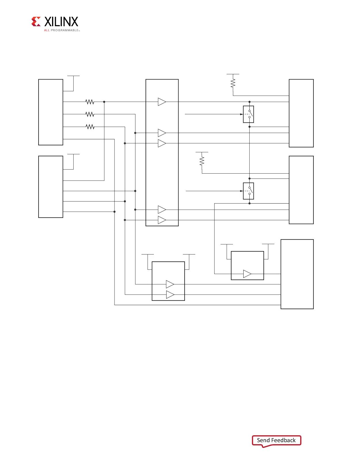
configures the FPGA with a temporary design to access and program the BPI or Quad SPI
flash memory device. The JTAG circuit is shown in Figure 1-9.
X-Ref Target - Fig ure 1-9
Figure 1-9: JTAG Circuit
UG810_c1_09_031214
JTAG_TDI
FMC_TDI_BUF
FPGA_TMS_BUF
FPGA_TDO
FPGA_TCK_BUF
FMC_LPC_TCK_BUF
FMC_HPC_TDO
FMC_LPC_TDO
FMC_TMS_BUF
LPC_PRSNT_M2C_B
HPC_PRSNT_M2C_B
JTAG_TMS
JTAG_TCK
JTAG_TDO
FMC_LPC_TMS_BUF
FMC_HPC_TCK_BUF
FMC_HPC_PRSNT_M2C_B
FMC_LPC_PRSNT_M2C_B
FMC HPC
Connector
TDI
TDO
J22
TMS
TCK
PRSNT_L
VCC3V3
FMC LPC
Connector
TDI
TDO
J2
TMS
TCK
PRSNT_L
Kintex-7
FPGA
TDI
TDO
U1
TMS
TCK
Digilent
USB-JTAG
Module
TMS
TDI
SN74AVC1T45
Voltage
Translator
U102
SN74AVC2T45
Voltage
Translator
U69
SN74LV541A
Voltage
Translator
U5
R381 15Ω
U59
R382 15Ω
R380 15Ω
TCK
TDO
TMS
TDI
J60
TCK
TDO
JTAG
Header
VCC2V5
VCC2V5
VCC3V3
VCC3V3
VCC3V3
VCC3V3
VCC3V3
U76
U77