KC705 Evaluation Board 59
UG810 (v1.8) March 20, 2018 www.xilinx.com
Chapter 1: KC705 Evaluation Board Features
GPIO SMA Connectors
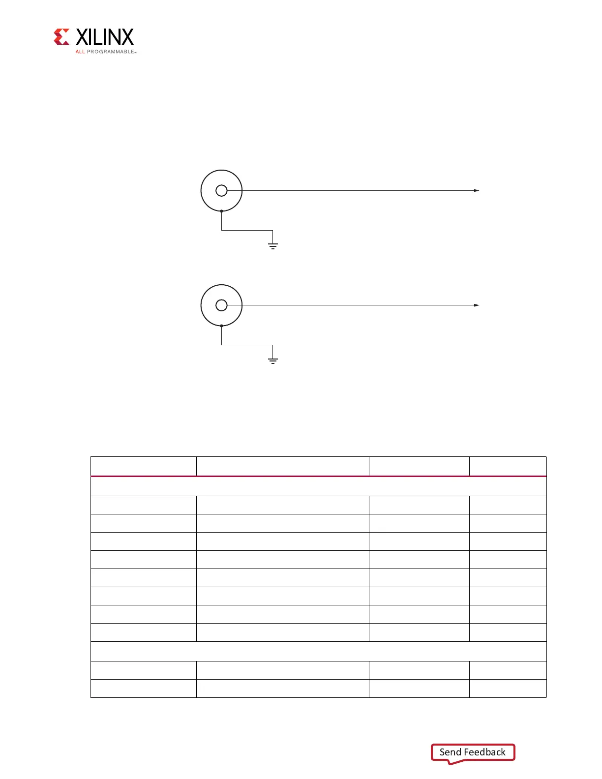
Figure 1-30 shows the GPIO SMAs J13 and J14.
[Figure 1-2, callout 26]
Table 1-27 lists the GPIO Connections to FPGA U1.
X-Ref Target - Figure 1-30
Figure 1-30: GPIO SMAs J13 and J14
Table 1-27: GPIO Connections to FPGA U1
U1 FPGA Pin Schematic Net Name I/O Standard GPIO Pin
Indicator LEDs (Active High)
AB8 GPIO_LED_0 LVCMOS15 DS4.2
AA8 GPIO_LED_1 LVCMOS15 DS1.2
AC9 GPIO_LED_2 LVCMOS15 DS10.2
AB9 GPIO_LED_3 LVCMOS15 DS2.2
AE26 GPIO_LED_4 LVCMOS25 DS3.2
G19 GPIO_LED_5 LVCMOS25 DS25.2
E18 GPIO_LED_6 LVCMOS25 DS26.2
F16 GPIO_LED_7 LVCMOS25 DS27.2
Directional Pushbutton Switches
AA12 GPIO_SW_N LVCMOS15 SW2.1
AG5 GPIO_SW_E LVCMOS15 SW3.1
GND
UG885_c1_30_031214
USER SMA GPIO P
J13
SMA
Connector
GND
USER SMA GPIO N
J14
SMA
Connector