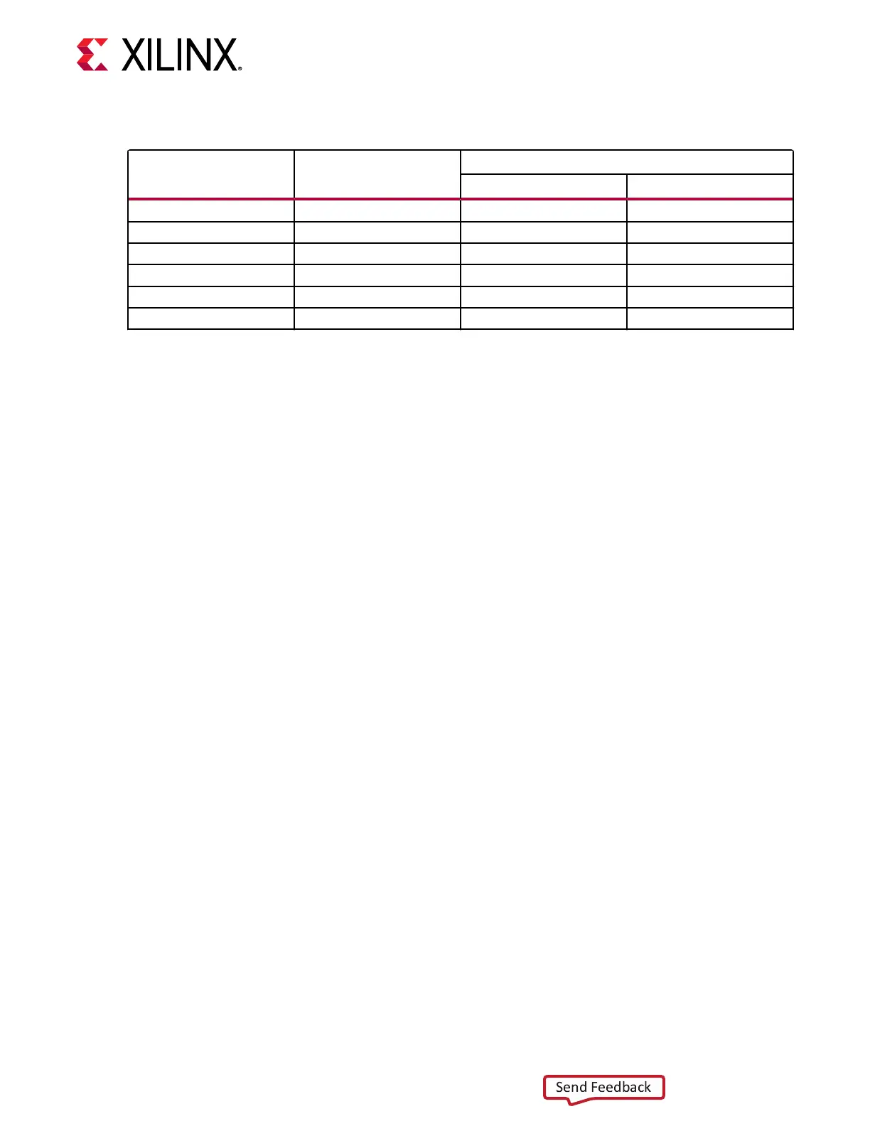
Table 9: Quad-SPI Component Connections to FPGA U1
XCVC37P (U1) Pin Net Name
U46 Quad SPI
Pin # Pin Name
AW15 QSPI_DQ0 D3 DQ0
AY15 QSPI_DQ1 D2 DQ1
AY14 QSPI_DQ2 C4 DQ2_W_B
AY13 QSPI_DQ3 D4 DQ3_RST_HLD_B
BD14 QSPI _CLK B2 C
BC15 QSPI_CS_B C2 S_B
The UltraScale Architecture Conguraon User Guide (UG570) provides FPGA conguraon details.
For more Quad SPI component informaon, see the Micron MT25QU02GCBB8E12-0SIT data
sheet at the Micron Technology website.
USB JTAG Interface
[Figure 2, callout 24]
JTAG conguraon is provided through a dual-funcon FTDI FT4232HL USB-to-JTAG/UART
bridge device (U8) where a host computer accesses the VCU128 board JTAG chain through a
type-A (PC host side) to micro-AB (VCU128 board side J2) USB cable.
A 2 mm JTAG header (J4) is also provided in parallel for access by Xilinx
®
download cables, such
as the Plaorm Cable USB II. JTAG iniated conguraon takes priority over the conguraon
method selected through the FPGA mode pins M[2:0], wired to SW1 posions [2:4]. The JTAG
chain of the VCU128 board is shown in the following gure.
Chapter 3: Board Component Descriptions
UG1302 (v1.0) December 21, 2018 www.xilinx.com
VCU128 Board User Guide 35