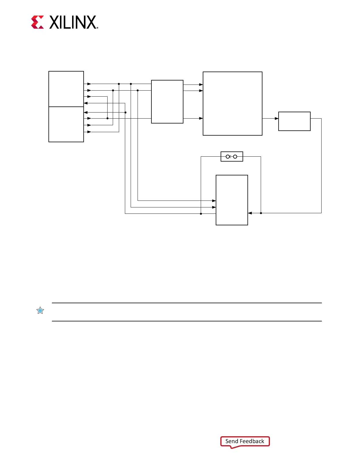
Figure 8: JTAG Chain Block Diagram
FTDI
USB
JTAG
(U8)
TCK
TMS
TDI
TDO
JTAG
2 mm
Conn.
(J4)
TDO
TDI
TMS
TCK
Level-shift
FPGA
Level-shift
1.8V3.3V
TCK
TMS
TDI TDO
1.8V 3.3V
U50
U1
U75
FMC+
HSPC
Connector
TMS
TCK
TDO
TDI
SPST Bus Switch
U72
J18
N.C.
X21649-110618
FMCP Connector JTAG Bypass
When an FMC is aached to the VCU128 board FMC+ HSPC connector J18, it is automacally
added to the JTAG chain through the electronically controlled single-pole single-throw (SPST)
switch U72. The SPST switch is in a normally closed state and transions to an open state when
the FMC is aached. Switch U72 adds an aached FMC to the FPGA JTAG chain as determined
by the FMCP_HSPC_PRSNT_M2C_B signal.
IMPORTANT
! The aached FMC must implement a TDI-to-TDO connecon through a device or
bypass jumper to ensure that the JTAG chain connects to the FPGA U1.
The JTAG connecvity on the VCU128 board allows a host computer to download bitstreams to
the FPGA using the Xilinx
®
tools. In addion, the JTAG connector allows debug tools such as the
Vivado
®
serial I/O analyzer or a soware debugger to access the FPGA. The Xilinx tools can also
program the Quad SPI ash memory.
Chapter 3: Board Component Descriptions
UG1302 (v1.0) December 21, 2018 www.xilinx.com
VCU128 Board User Guide 36