Clock Generation
[Figure 2, callout 10-18]
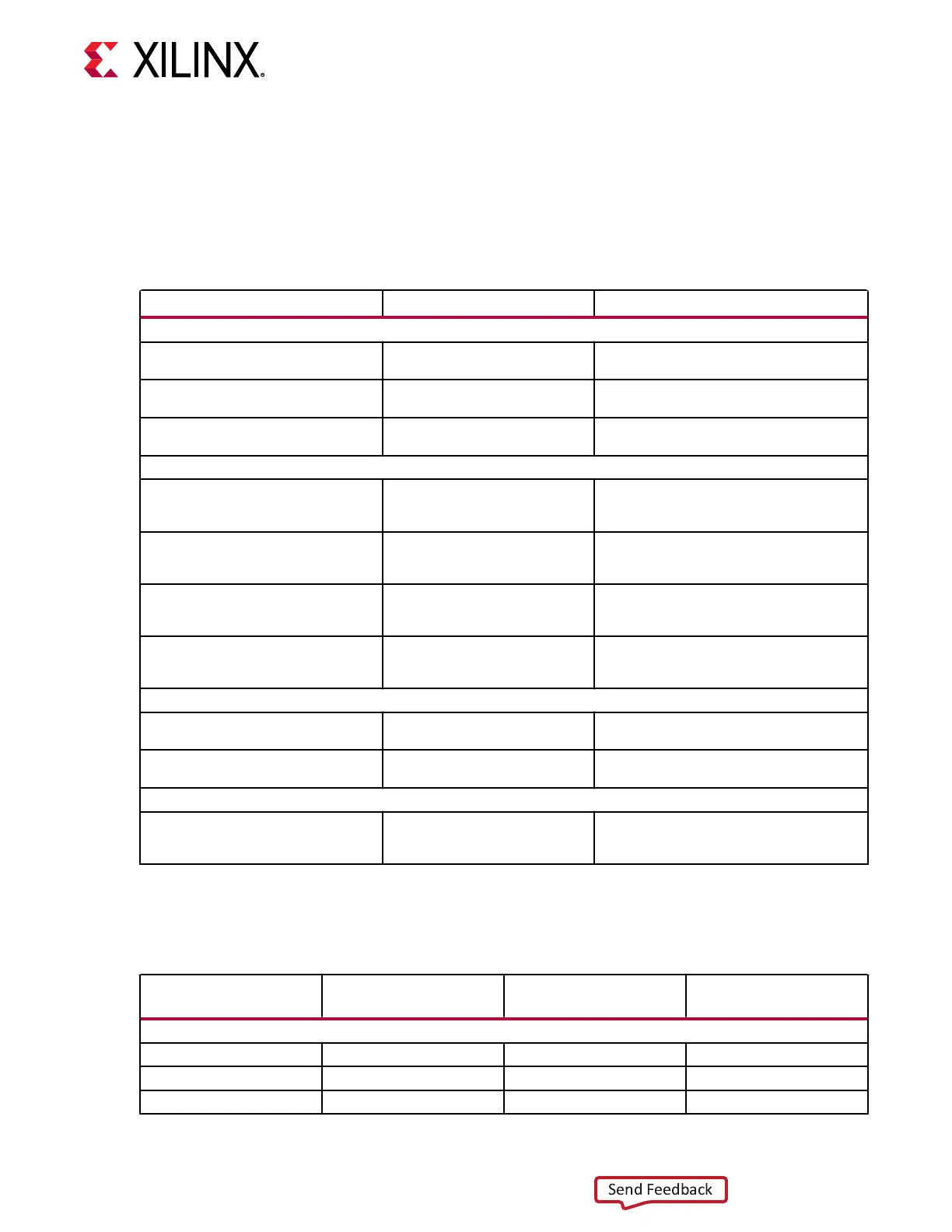
The VCU128 evaluaon board clock sources to the FPGA are listed in the following table.
Table 10: Board Clock Sources
Clock Name Clock Ref. Des. Description
Memory Interface Clocks
DDR4 clock 100 MHz U76 SiTime SiT9120AI 3.3V fixed frequency
100.000 MHz (DDR4_CLK_100MHZ_P/N)
QDR4 clock 100 MHz U96 SiTime SiT9120AI 3.3V fixed frequency
100.000 MHz (QDR4_CLK_100MHZ_P/N)
RLD3 clock 100 MHz U45 SiTime SiT9120AI 3.3V fixed frequency
100.000 MHz (RLD3_CLK_100MHZ_P/N)
QSFP Interface Clocks
QSFP1 clock 156.250 MHz U95 Silicon Labs Si570 3.3V LVDS I2C
programmable oscillator, 156.250 MHz
default. (QSFP1_SI570_CLOCK_P/N)
QSFP2 clock 156.250 MHz U90 Silicon Labs Si570 3.3V LVDS I2C
programmable oscillator, 156.250 MHz
default. (QSFP2_SI570_CLOCK_P/N)
QSFP3 clock 156.250 MHz U82 Silicon Labs Si570 3.3V LVDS I2C
programmable oscillator, 156.250 MHz
default. (QSFP3_SI570_CLOCK_P/N)
QSFP4 clock 156.250 MHz U80 Silicon Labs Si570 3.3V LVDS I2C
programmable oscillator, 156.250 MHz
default. (QSFP4_SI570_CLOCK_P/N)
SMA GTY REFCLK and User Clock
QSFP GTY131 REFCLK1 SMA clock SMA J24 (P)/SMA J26 (N) Bank 131 series capacitor coupled SMA clock
(SMA_REFCLK_INPUT_P/N)
FPGA U1 bank 67 GPIO user SMA clock SMA J12 (P)/SMA J13 (N) Bank 67 QBC direct connect GPIO
SMA )SMA_CLK_OUTPUT_P/N)
QSFP1/2 recovery clocks
QSFP1/2 jitter attenuated clock U87 Silicon Labs Si5328B LVDS precision clock,
multiplier/jitter attenuator. See Jitter
Attenuated Clock (SI5328_CLOCK1/2_P/N)
The following table lists the VCU128 clock sources-to-FPGA U1 connecons.
Table 11: Clock Sources to XCVU37P FPGA U1 Connections
Clock Source Device/
U#.Pin#
Schematic Net Name I/O Standard FPGA (U1) Pin
Memory Interface Clocks
SIT9120AI/U76.4 DDR4_CLK_100MHZ_P LVDS BH51
SIT9120AI/U76.5 DDR4_CLK_100MHZ_N LVDS BJ51
SIT9120AI/U96.4 QDR4_CLK_100MHZ_P LVDS BJ4
Chapter 3: Board Component Descriptions
UG1302 (v1.0) December 21, 2018 www.xilinx.com
VCU128 Board User Guide 38