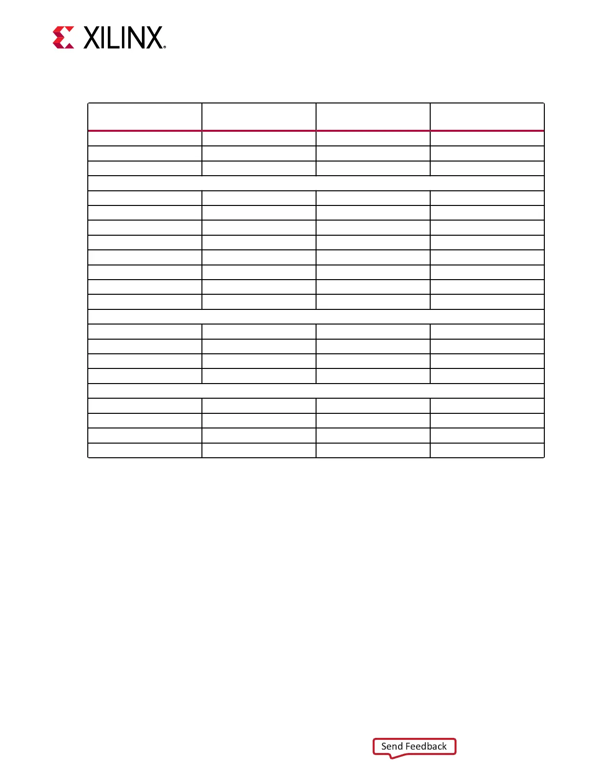
Table 11: Clock Sources to XCVU37P FPGA U1 Connections (cont'd)
Clock Source Device/
U#.Pin#
Schematic Net Name I/O Standard FPGA (U1) Pin
SIT9120AI/U96.5 QDR4_CLK_100MHZ_N LVDS BK3
SIT9120AI/U45.4 RLD3_CLK_100MHZ_P LVDS F35
SIT9120AI/U45.5 RLD3_CLK_100MHZ_N LVDS F36
QSFP Interface Clocks
SI570/U95.4 QSFP1_SI570_CLOCK_P
1
P42
SI570/U95.5 QSFP1_SI570_CLOCK_N
1
P43
SI570/U90.4 QSFP2_SI570_CLOCK_P
1
T42
SI570/U90.5 QSFP2_SI570_CLOCK_N
1
T43
SI570/U82.4 QSFP3_SI570_CLOCK_P
1
Y42
SI570/U82.5 QSFP3_SI570_CLOCK_N
1
Y43
SI570/U80.4 QSFP4_SI570_CLOCK_P
1
AB42
SI570/U80.5 QSFP4_SI570_CLOCK_N
1
AB43
SMA GTY REFCLK and User Clock
SMA J24.1 SMA_REFCLK_INPUT_P
1
AA40
SMA J26.1 SMA_REFCLK_INPUT_N
1
AA41
SMA J12.1 SMA_CLK_OUTPUT_P
2
BK26
SMA J13.1 SMA_CLK_OUTPUT_N
2
BL25
QSFP1/2 Recovery Clocks
SI5328B/U87.29 SI5328_CLOCK1_P
1
R40
SI5328B/U87.28 SI5328_CLOCK1_P
1
R41
SI5328B/U87.35 SI5328_CLOCK2_P
1
W40
SI5328B/U87.34 SI5328_CLOCK2_P
1
W41
Notes:
1. Series capacitor coupled, MGT connections I/O standard is not applicable.
2. Signal amplitude not to exceed FPGA U1 bank 67 VCCO = VCC1V8 rail = 1.8V.
Chapter 3: Board Component Descriptions
UG1302 (v1.0) December 21, 2018 www.xilinx.com
VCU128 Board User Guide 39