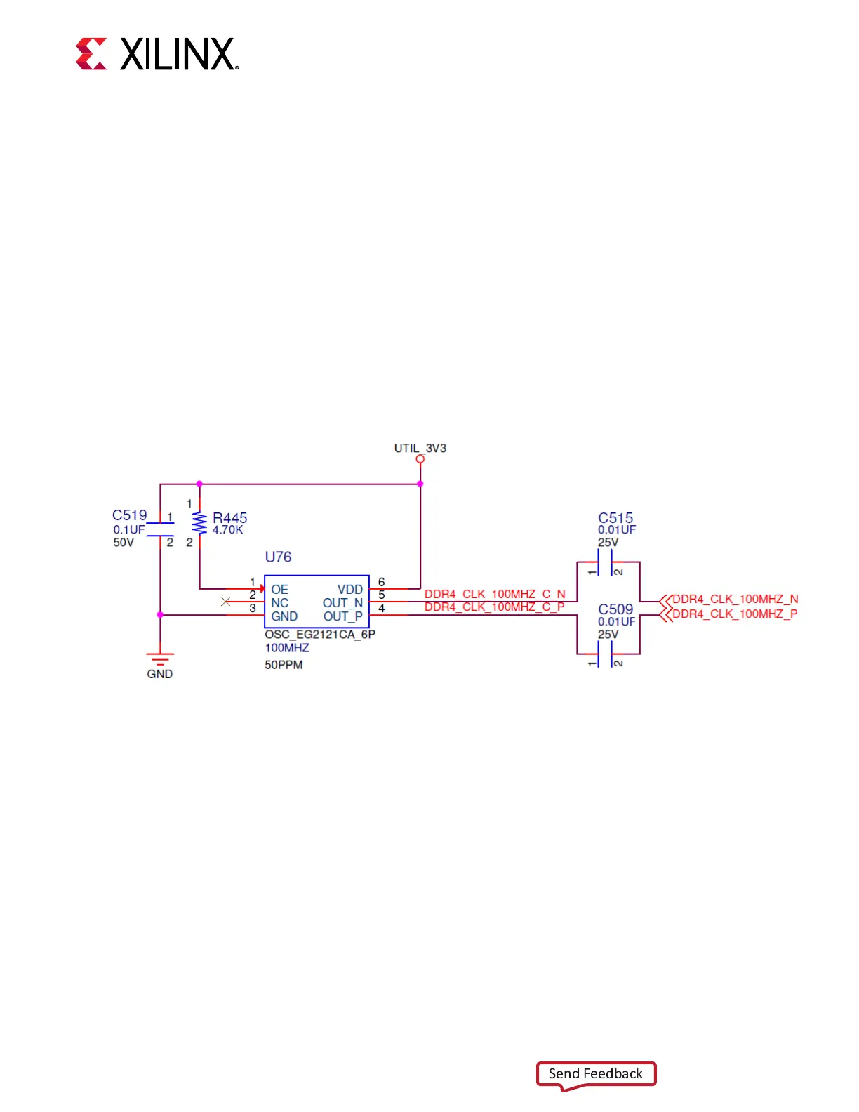
DDR4 Interface Clock
[Figure 2, callout 10]
The VCU128 evaluaon board has a SiTime 100 MHz xed frequency low-jier 3.3V LVDS
dierenal oscillator (U76) connected to FPGA U1 HP bank 66 DDR4 interface GC pins BH51
(P) and BJ51 (N) and is series capacitor coupled.
• Fixed frequency oscillator: SiTime SIT9120AI-2D3-33E100.0000 (100 MHz)
• 0.6 ps RMS phase jier (random) over 12 kHz to 20 MHz bandwidth
• 3.3V LVDS dierenal output
The DDR4 interface xed frequency clock circuit is shown in the following gure.
Figure 10: DDR4 Interface Clock
X21959-121918
Chapter 3: Board Component Descriptions
UG1302 (v1.0) December 21, 2018 www.xilinx.com
VCU128 Board User Guide 40