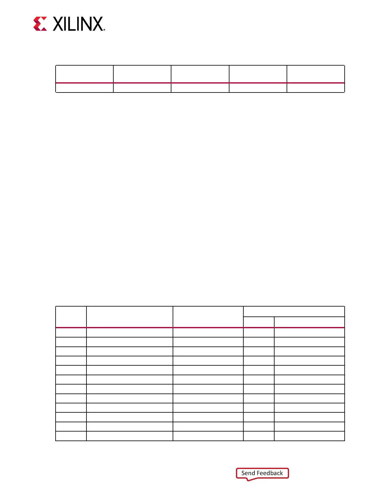
Table 26: XCVU37P U1 to QSFP28 Module Control and I2C Connections (cont'd)
FPGA (U1) Pin
Schematic Net
Name
1
,
2
FPGA (U1)
Direction
Module Pin Num Module Pin Name
U54.20 QSFP4_I2C_SCL Output 11 SCL
Notes:
1. The QSFP28 connector control signals are level-shifted.
2. The four QSFP28 connector I2C SCL/SDA signals are connected via I2C switch U54 to the I2C1_SCL/SDA bus. See I2C
Bus, Topology, and Switches section
For addional informaon about the quad small form factor pluggable (28 Gb/s QSFP28) module,
see the SFF-8663 and SFF-8679 specicaons for the 28 Gb/s QSFP+ on the SNIA Technology
Aliates website.
10/100/1000 Mb/s Tri-speed Ethernet PHY
[Figure 2, callout 22]
The VCU128 evaluaon board uses the TI PHY device DP83867ISRGZ (U62) for Ethernet
communicaons at 10 Mb/s, 100 Mb/s, or 1000 Mb/s. The board supports SGMII mode only.
The PHY connecon to a user-provided Ethernet cable is through RJ-45 connector P2, a Wurth
7499111221A with built-in magnecs and status LEDs. On power-up, or on reset, the PHY is
congured to operate in SGMII mode with PHY address[4:0] = 00011. The following table lists
the FPGA U1 to U62 DP83867ISRGZ Ethernet PHY connecons. This table also shows the net
names for the connecons from the FPGA to the Ethernet PHY. ENET_SGMII_IN correlates with
the SGMII_TX ports in the FPGA design, and ENET_SGMII_OUT correlates with the SGMII_RX
ports.
Table 27: XCVC37P U1 to Ethernet PHY U62 Connections
FPGA
(U1) Pin
Net Name I/O Standard
DP83867ISRGZ U62
Pin Name
BG23 ENET_MDIO LVCMOS18 17 MDIO
BN27 ENET_MDC LVCMOS18 16 MDC
BF22 ENET_PDWN_B_I_INT_B_O LVCMOS18 44 INT_PWDN
BH22 ENET_SGMII_IN_N LVCMOS18 28 TX_D1_SGMII_SIP
BG22 ENET_SGMII_IN_P LVCMOS18 27 TX_D0_SGMII_SIN
BJ21 ENET_SGMII_OUT_N LVCMOS18 36 RX_D3_SGMII_SON
BH21 ENET_SGMII_OUT_P LVCMOS18 35 RX_D2_SGMII_SOP
BK22 ENET_SGMII_CLK_N LVCMOS18 34 RX_D1_SGMII_CON
BK23 ENET_SGMII_CLK_P LVCMOS18 33 RX_D0_SGMII_COP
U65.10 GEM3_ENET_RESET_B NA 43 RESET_B
BP27 ENET_COL_GPIO LVCMOS18 39 GPIO_2
BJ23 ENET_CLKOUT LVCMOS18 18 CLK_OUT
Chapter 3: Board Component Descriptions
UG1302 (v1.0) December 21, 2018 www.xilinx.com
VCU128 Board User Guide 71