X21976-112818
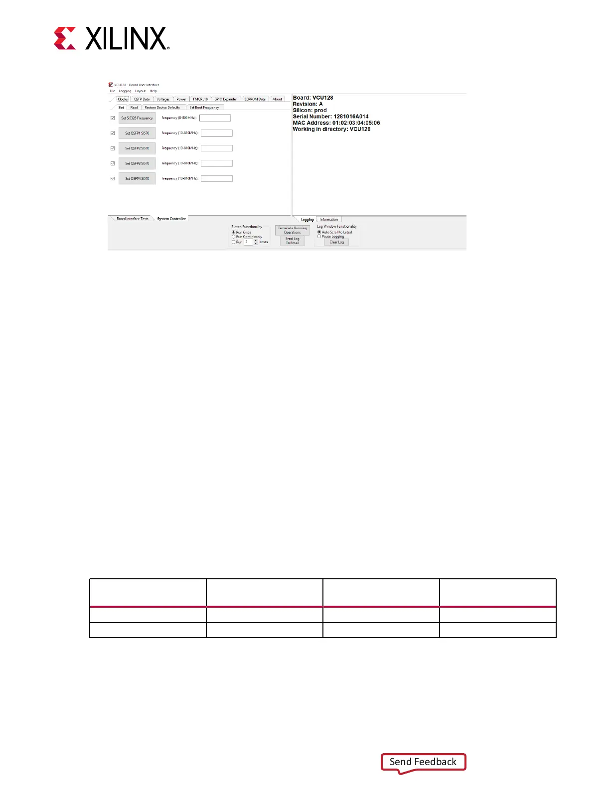
See the VCU128 System Controller Tutorial (XTP534) and the VCU128 Soware Install and Board
Setup Tutorial (XTP535) for more informaon on installing and using the System Controller ulity.
Configuration Options
[Figure 2, callout 36]
The VCU128 board supports two of the seven UltraScale™ FPGA conguraon modes.
• Master SPI using the onboard 2 Gbit Quad SPI ash memory
• JTAG using:
○ USB JTAG conguraon port J2 (FTDI FT4232H bridge U8)
○ Xilinx
®
plaorm cable 2 mm, keyed at cable header (J4)
Each conguraon interface corresponds to one or more conguraon modes and bus widths as
listed in the following table. The mode switches M2, M1, and M0 are on 4-pole DIP SW1
posions 2, 3, and 4, respecvely. The FPGA default mode seng M[2:0] = 001, selecng the
master SPI conguraon mode.
Table 34: Board FPGA Configuration Modes
Configuration Mode
SW16 DIP Switch
Settings (M[2:0])
Bus Width CCLK Direction
Master SPI 1 x1, x2, x4 Output
JTAG 101 x1 Not applicable
The following gure shows mode switch SW1.
Chapter 3: Board Component Descriptions
UG1302 (v1.0) December 21, 2018 www.xilinx.com
VCU128 Board User Guide 91