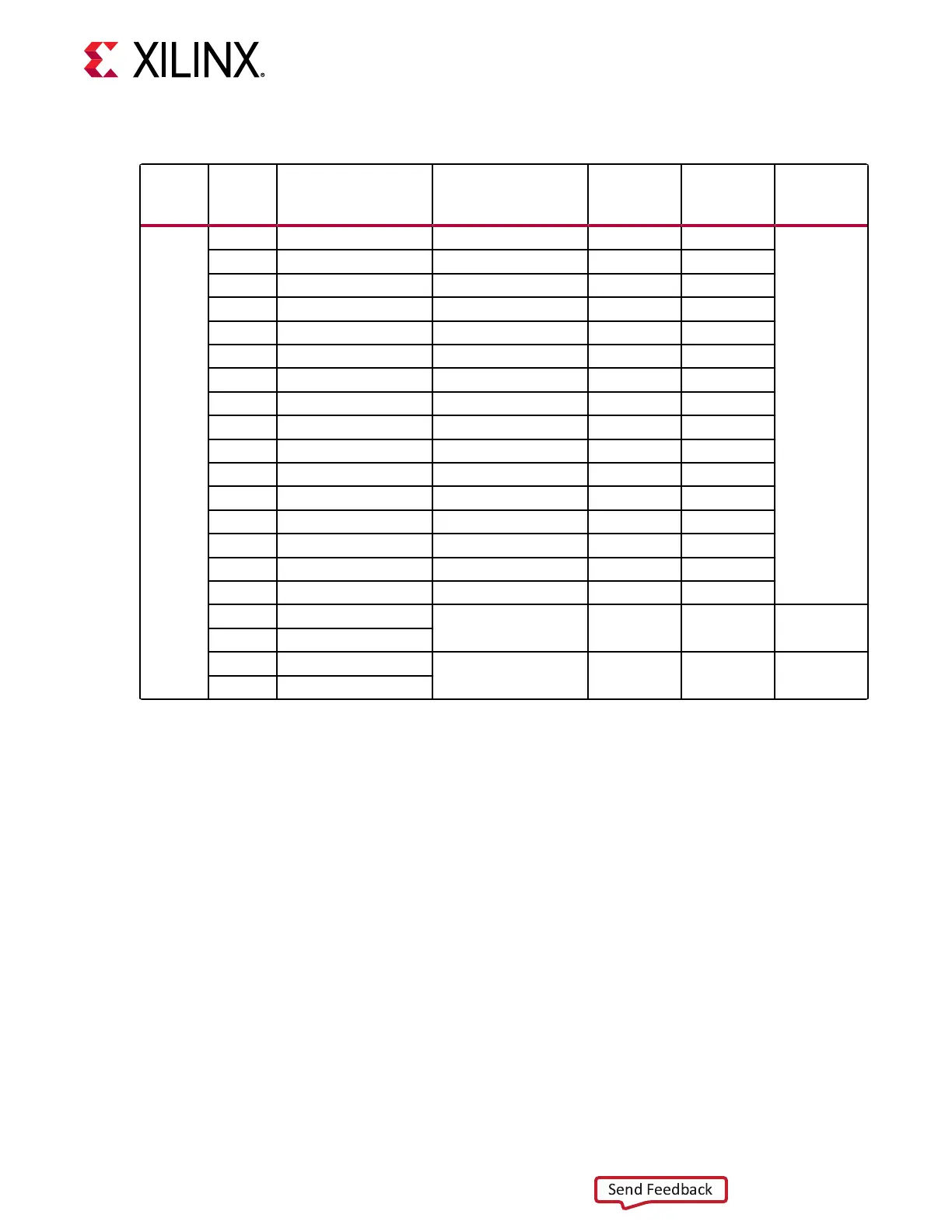
Table 25: XCVU37P U1 GTY Transceiver Bank 224 Connections
MGT
bank
FPGA
(U1)
Pin
FPGA (U1) Pin
Name
Schematic Net
Name TX
Connected
Pin
Connected
Pin Name
Connected
device
GTY bank
224
BC7 MGTYTXP0_224 PCIE_TX15_P A80 PERP15
PCIE 16-lane
edge conn. P1
BC6
MGTYTXN0_224 PCIE_TX15_N A81 PERN15
BC2 MGTYRXP0_224 PCIE_RX15_P B78 PETP15
BC1 MGTYRXN0_224 PCIE_RX15_N B79 PETN15
BC11 MGTYTXP1_224 PCIE_TX14_P A76 PERP14
BC10 MGTYTXN1_224 PCIE_TX14_N A77 PERN14
BB4 MGTYRXP1_224 PCIE_RX14_P B74 PETP14
BB3 MGTYRXN1_224 PCIE_RX14_N B75 PETN14
BB9 MGTYTXP2_224 PCIE_TX13_P A72 PERP13
BB8 MGTYTXN2_224 PCIE_TX13_N A73 PERN13
BA2 MGTYRXP2_224 PCIE_RX13_P B70 PETP13
BA1 MGTYRXN2_224 PCIE_RX13_N B71 PETN13
BA11 MGTYTXP3_224 PCIE_TX12_P A68 PERP12
BA10 MGTYTXN3_224 PCIE_TX12_N A69 PERN12
BA6 MGTYRXP3_224 PCIE_RX12_P B66 PETP12
BA5 MGTYRXN3_224 PCIE_RX12_N B67 PETN12
AV13 MGTREFCLK0P_224
NC NC NC NC
AV12 MGTREFCLK0N_224
AT13 MGTREFCLK1P_224
NC NC NC NC
AT12 MGTREFCLK1N_224
Notes:
1. Series 0.01uF capacitor coupled.
PCI Express Endpoint Connectivity
[Figure 2, callout 20]
The 16-lane PCI Express
®
edge connector P1 performs data transfers at the rate of 2.5 GT/s for
Gen1 applicaons, 5.0 GT/s for Gen2 applicaons, 8.0 GT/s for Gen3 applicaons and 16.0 GT/s
for Gen4 applicaons. The PCIe
®
transmit and receive signal data paths have a characterisc
impedance of 85Ω ±10%. The PCIe clock is routed as a 100Ω dierenal pair.
Chapter 3: Board Component Descriptions
UG1302 (v1.0) December 21, 2018 www.xilinx.com
VCU128 Board User Guide 67