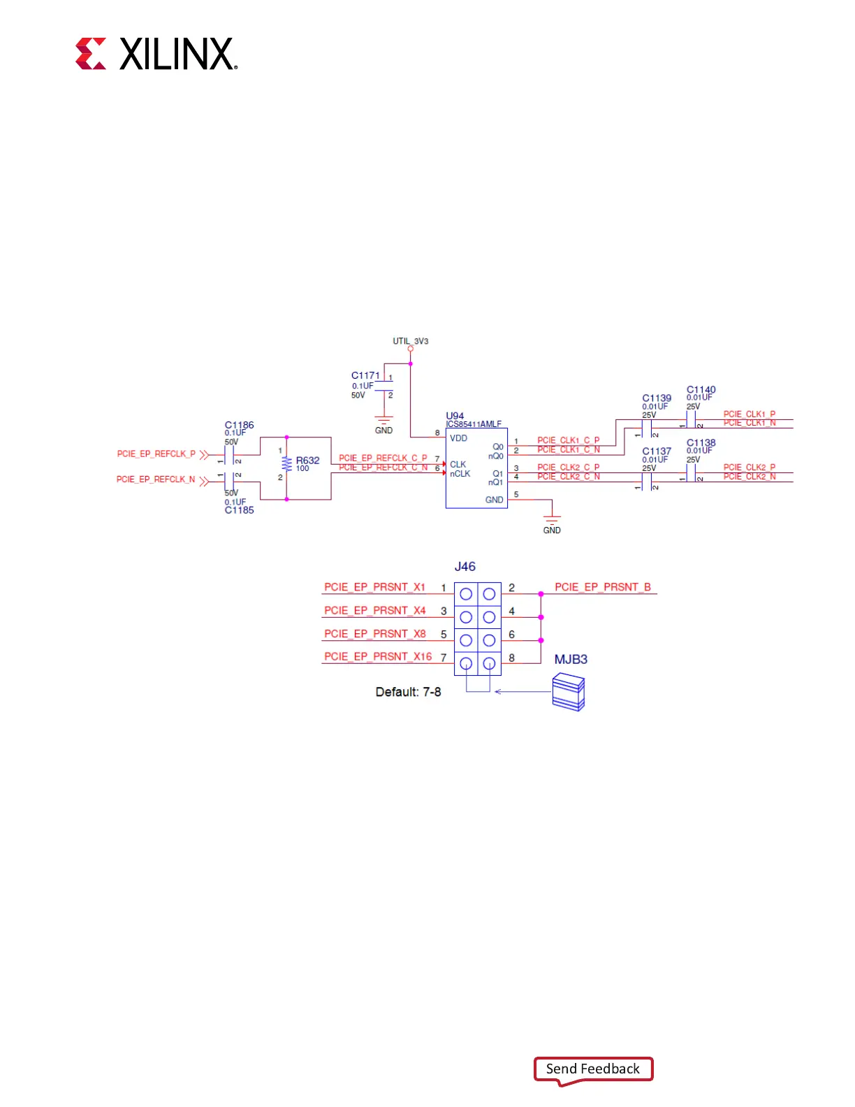
The XCVU37P-2FSVH2892E (-2 speed grade) is deployed on the VCU128 to support up to Gen4
x8. User selectable as PCIe Gen3 x16 or dual Gen4 x8. The PCIe reference clock is input from the
P1 edge connector. The PCIe clock is routed from P1 pin A16 (P) and pin A17 (N) to a 1-to-2
ICS85411A clock buer U94. The Q0 output of U94 is wired to the GTY225 MGTHREFCLK0
input (see Table 24). The Q1 output of U94 is wired to the GTY227 MGTHREFCLK0 input (see
Table 22). PCIe lane width/size is selected by jumper J46. The default lane size selecon is 16-
lane (J46 pins 7 and 8 jumpered). The 1-to-2 U94 PCIe clock buer circuit and J46 lane size
jumper are shown in the following gure.
Figure 22: PCI Express Lane Clock Circuit and Size Select Jumper J46
X21969-112818
The tables in Le-side GTY Transceiver Connecvity list the PCIe P1 edge connector wiring to
the XCVU37P FPGA U1 MGTY transceiver banks 227-224. The two PCIe P1 edge connector
control signals PCIE_EP_WAKE (P1 pin B11) and PCIE_EP_PERST (P1 pin A11) are level-shied
by SN74AVC2T245 U70 and connected to the XCVU39P U1 bank 65 pin BJ42 and pin BF41,
respecvely. For addional informaon about UltraScale™ PCIe funconality, see the UltraScale
Devices Gen3 Integrated Block for PCI Express LogiCORE IP Product Guide (PG156). Addional
informaon about the PCI Express standard is available on the PCI Express standard website.
Chapter 3: Board Component Descriptions
UG1302 (v1.0) December 21, 2018 www.xilinx.com
VCU128 Board User Guide 68