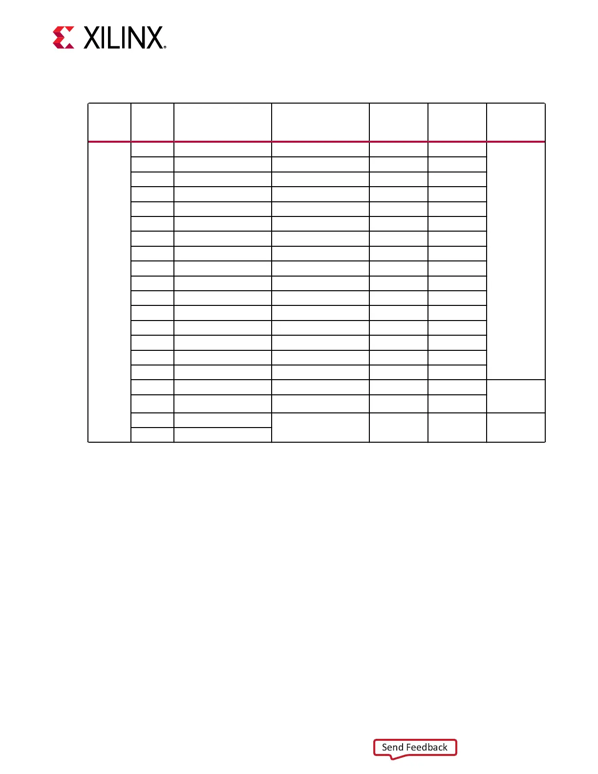
Table 22: XCVU37P U1 GTY Transceiver Bank 227 Connections
MGT
Bank
FPGA
(U1)
Pin
FPGA (U1) Pin
Name
Schematic Net
Name TX
1
Connected
Pin
Connected
Pin Name
Connected
Device
GTY bank
227
AP9 MGTYTXP0_227 PCIE_EP_TX3_P A29 PERP3
PCIE 16-lane
edge conn. P1
AP8
MGTYTXN0_227 PCIE_EP_TX3_N A30 PERN3
AN2 MGTYRXP0_227 PCIE_EP_RX3_P B27 PETP3
AN1 MGTYRXN0_227 PCIE_EP_RX3_N B28 PETN3
AN11 MGTYTXP1_227 PCIE_EP_TX2_P A25 PERP2
AN10 MGTYTXN1_227 PCIE_EP_TX2_N A26 PERN2
AN6 MGTYRXP1_227 PCIE_EP_RX2_P B23 PETP2
AN5 MGTYRXN1_227 PCIE_EP_RX2_N B24 PETN2
AM9 MGTYTXP2_227 PCIE_EP_TX1_P A21 PERP1
AM8 MGTYTXN2_227 PCIE_EP_TX1_N A22 PERN1
AM4 MGTYRXP2_227 PCIE_EP_RX1_P B19 PETP1
AM3 MGTYRXN2_227 PCIE_EP_RX1_N B20 PETN1
AL11 MGTYTXP3_227 PCIE_EP_TX0_P A16 PERP0
AL10 MGTYTXN3_227 PCIE_EP_TX0_N A17 PERN0
AL2 MGTYRXP3_227 PCIE_EP_RX0_P B14 PETP0
AL1 MGTYRXN3_227 PCIE_EP_RX0_N B15 PETN0
AL15 MGTREFCLK0P_227 PCIE_CLK2_P
1
3 Q1 ICS85411A
U94 clock
buffer
AL14 MGTREFCLK0N_227 PCIE_CLK2_N
1
4 NQ1
AK13 MGTREFCLK1P_227
NC NC NC NC
AK12 MGTREFCLK1N_227
Notes:
1. Series 0.01uF capacitor coupled.
Chapter 3: Board Component Descriptions
UG1302 (v1.0) December 21, 2018 www.xilinx.com
VCU128 Board User Guide 64