Pin
No.
Port Name
Function Name
(P.C.B.)
I/O
Detail of Function
PowerOn
Standby
MCUSleep
EEP Writing
[When writing]
34 P6_4/nCTS1/nRTS1/nCTS0/
CLKS1
WR_BUSY O O O [MCU] For simple emulation / BUSY output when writing flash
35 P6_3/TXD0/SDA0 DAC_SDA SO O O DAC ESS9018S control I2C data input/output / I2C fs=100k/400k
36 P6_2/RXD0/SCL0 DAC_SCL SO O O DAC ESS9018S control I2C data output / I2C fs=100k/400k
37 P6_1/CLK0 DAC_N_RST O O O DAC ESS9018S control reset output
38 P6_0/RTCOUT/nCTS0/nRTS0 TROPEN_SW I O O LOADER tray open detection
39 P5_7/nRDY/CLKOUT TRCLOSE_SW I O O LOADER tray close detection
40 P5_6/ALE TRAY_SW I O O LOADER tray detection
41 P5_5/nHOLD STBY_CNT/N_EMP I, O O O For flash writing (IO)
BOOT mode: P5_5=L, CNVSS=H, P5_0=H
Set to Pull-down as Hiz state may occur during emulator operation.
• +5SPC power ONOFF control
(L=OFF, H=ON: For reduction of stand-by power)
• Usually fixed at Low standby power is reduced (MCUSleep) by
setting to Low after processing required for standby state.
When shifting to the stand-by state, set to Low after completion
procedure
42 P5_4/nHLDA TRAY_MTR2 O O O Tray motor control
43 P5_3/BCLK TRAY_MTR1 O O O Tray motor control
44 P5_2/nRD CLAMP_MTR2 O O O Clamper control
45 P5_1/nWRH/nBHE CLAMP_MTR1 O O O Clamper control
46 P5_0/nWRL/nWR
UNCLAMP_SW/N_CE
I O O For flash writing (HI)
BOOT mode: P5-5=L, CNVSS=H, P5_0=H / Clamper detection
47 P4_7/PWM1/TXD7/SDA7/nCS3 FPGA_INITN I O O Readiness for FPGA/GPLD configuration is indicated
PU is enabled during configuration in FPGA
48 P4_6/PWM0/RXD7/SCL7/nCS2 FPGA_DONE I O O FPGA Config DONE input
Completion of configuration sequence and starting sequence
going on are indicated
49 P4_5/CLK7/nCS1 FPGA_PROG O O O FPGA Config starting / Configuration started at L
Note: Do not apply trigger to the device when DONE is at Low
50 P4_4/nCTS7/nRTS7/nCS0 CLAMP_SW I O O Clamper detection
51 P4_3/A19 FPGA_SELC O O O FPGA sound output selection / Designated with 3 bit
52 P4_2/A18 FPGA_SELB O O O FPGA sound output selection / Designated with 3 bit
53 P4_1/A17 FPGA_SELA I O O FPGA sound output selection / Designated with 3 bit
54 P4_0/A16 SSP2_YOSI_MUTE I O O USB streaming controller TE8802 control / Output resolutions
0: 16bit, 1: 24bit
55 P3_7/A15 SSP2_N_DSPSTOP I O O USB streaming controller SSP2 control
DSP function unavailable
56 P3_6/A14 SSP2_DSD_PCM I O O USB streaming controller SSP2 control
DSD/PCM status input from driver via SSP2
57 P3_5/A13 SSP2_YISO_MUTE I O O USB streaming controller SSP2 control
MUTE request input due to SSP2 error
58 P3_4/A12 SSP2_USB_RDY I O O USB streaming controller SSP2 control / USB ready state input
Whether USB available or not is judged
59 P3_3/A11 SSP2_N_IC O O O USB streaming controller SSP2 control IC output
60 P3_2/A10 SSP2_PON O O O USB streaming controller power control for SSP2 control
High=On, Low=Off
61 P3_1/A9 LED_PWR O O O LED_POWER control / H: On, L: Off
62 Vcc2 VCC2 MCU MCU MCU +5M
63 P3_0/A8 FPGA_RRESET O O O FPGA / Register reset
64 Vss VSS All MCU D_GND
65 P2_7/AN2_7/A7 DPWR_ON O O O Power for digital 33D, 15D 115D, VBUS On/Off
High: On, Low: Off
45
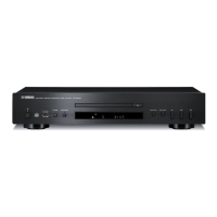
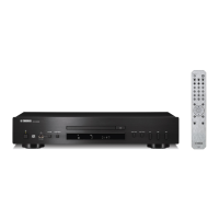
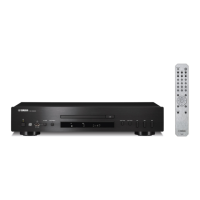
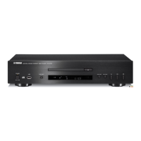
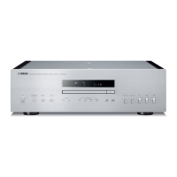
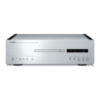
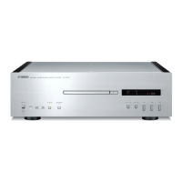
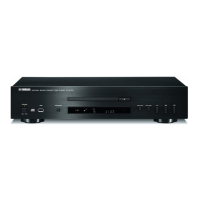
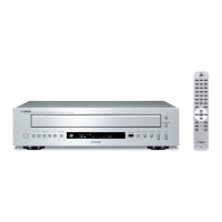
CD-S3000
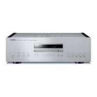
CD-S3000
 Loading...