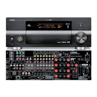
RX-V2400/RX-V2400RDS/DSP-AX2400
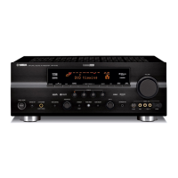
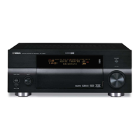
RX-V1400/RX-V1400RDS/HTR-5690/DSP-AX1400
RX-V2400/RX-V2400RDS/DSP-AX2400
RX-V1400/RX-V1400RDS/HTR-5690/DSP-AX1400
56
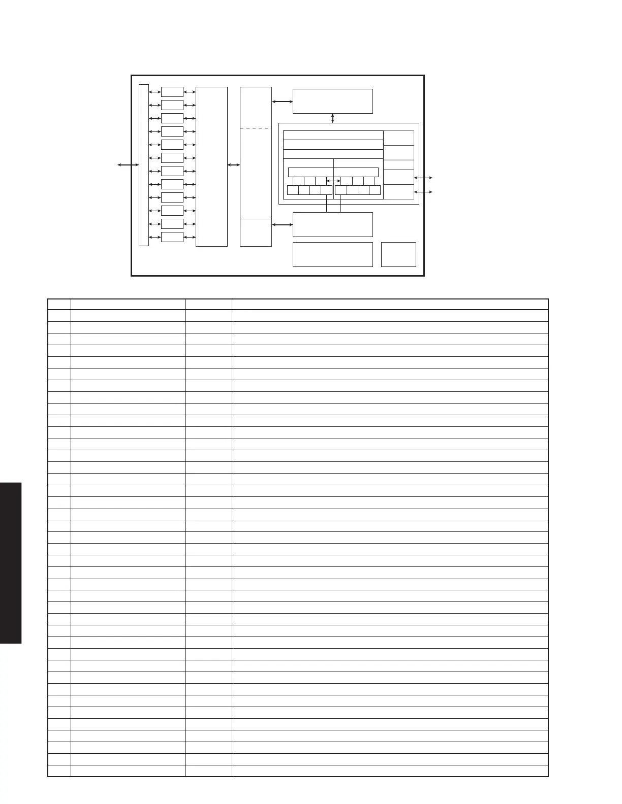
No. Name I/O Function
General purpose I/O0 port 4
General purpose I/O0 port 6
1.2V power supply
Ground
3.3V power supply
General purpose I/O0 port 5
General purpose I/O0 port 7
McBSP1 external clock source
3.3V power supply
Ground
1.2V power supply
Timer 1 Input
Timer 1 Output
1.2V power supply
Ground
McASP0 Transmission BCLK
Timer 0 Input
Timer 0 Output
McASP0 Reception BCLK
McASP0 Transmission/reception data 1
McASP0 Transmission LRCLK
1.2V power supply
Ground
McASP0 Reception LRCLK
3.3V power supply
Ground
McASP0 Transmission/reception data 0
McASP0 Reception MCLK
1.2V power supply
Ground
McBSP1 Transmission Frame Sync (Input in SPI slave state)
McBSP1 Transmission data
McBSP1 Transmission clock (Input in SPI slave state)
Ground
1.2V power supply
McBSP1 Reception clock
McBSP1 Reception data
McBSP1 Reception Frame Sync
Ground
1.2V power supply
IC512: D601A002PYP180 (DSP P.C.B)
Decoder
Pin Multiplexing
EMIF32
L1P Cache
Direct Mapped
4K Bytes Total
Digital Signal Processors
L1D Cache
2-Way Set
Associative
4K Bytes Total
Clock Generator,
Oscillator and PLL
x4 through x25 Multipliers
/1 through /32 Dividers
Power-Down
Logic
Instruction Fetch
Instruction Dispatch
Instruction Decode
Data Path BData Path A
B Register File
Control
Registers
C67x
TM
CPU
Control
Logic
In-Circuit
Emulation
Interrupt
Control
Test
A Register File
.L1t
McASP1
McASP0
McBSP1
McBSP0
I2C1
I2C0
Timer 1
Timer 0
.S1t .M1t .D1 .D2 .M2t .S2t .L2t
GP1
GP0
HPI16
Enhanced
DMA
Controller
(16 channel)
L2 Cache/
Memory
4 Banks
64K Bytes
To ta l
(4-Way)
L2
Memory
DA610:
192K Bytes
DA601:
64K Bytes
R2 ROM
512K
Bytes
To ta l
 Loading...