EasyManua.ls Logo

Yamaha HTR-5630RDS Service Manual

Yamaha HTR-5630RDS
79 pages
To Next Page IconTo Next Page
Page #1 background imageLoading...
Page #1 background image
SERVICE MANUAL
100848
IMPORTANT NOTICE
This manual has been provided for the use of authorized YAMAHA Retailers and their service personnel.
It has been assumed that basic service procedures inherent to the industry, and more specifically YAMAHA Products, are already
known and understood by the users, and have therefore not been restated.
WARNING: Failure to follow appropriate service and safety procedures when servicing this product may result in personal
injury, destruction of expensive components, and failure of the product to perform as specified. For these reasons,
we advise all YAMAHA product owners that any service required should be performed by an authorized
YAMAHA Retailer or the appointed service representative.
IMPORTANT: The presentation or sale of this manual to any individual or firm does not constitute authorization, certification or
recognition of any applicable technical capabilities, or establish a principle-agent relationship of any form.
The data provided is believed to be accurate and applicable to the unit(s) indicated on the cover. The research, engineering, and
service departments of YAMAHA are continually striving to improve YAMAHA products. Modifications are, therefore, inevitable
and specifications are subject to change without notice or obligation to retrofit. Should any discrepancy appear to exist, please
contact the distributor's Service Division.
WARNING: Static discharges can destroy expensive components. Discharge any static electricity your body may have
accumulated by grounding yourself to the ground buss in the unit (heavy gauge black wires connect to this buss).
IMPORTANT: Turn the unit OFF during disassembly and part replacement. Recheck all work before you apply power to the unit.
P.O.Box 1, Hamamatsu, Japan
CONTENTS
TO SERVICE PERSONNEL .......................................... 2
FRONT PANELS ........................................................ 3~4
REAR PANELS .......................................................... 4~7
REMOTE CONTROL PANELS...................................... 7
SPECIFICATIONS / 参考仕様 .................................. 8~11
INTERNAL VIEW ......................................................... 11
DISASSEMBLY PROCEDURES/分解手順 ......... 12~14
SELF DIAGNOSIS FUNCTION (DIAG)/
自己診断機能(ダイアグ)..................................... 15~35
CONFIRMATION OF IDLING CURRENT/
アイドリング電流の確認 .............................................. 36
DISPLAY DATA ..................................................... 37~38
IC DATA ................................................................. 39~44
PRINTED CIRCUIT BOARD .................................. 45~53
PIN CONNECTION DIAGRAM .................................... 54
BLOCK DIAGRAM ....................................................... 55
SCHEMATIC DIAGRAM ........................................ 56~60
PARTS LIST ........................................................... 61~79
REMOTE CONTROL.............................................. 80~81
AV RECEIVER/AV AMPLIFIER
RX-V340/RX-V340RDS/
HTR-5630/HTR-5630RDS/DSP-AX340
RX-V340/RX-V340RDS/
HTR-5630/HTR-5630RDS/DSP-AX340
w
w
w
.
x
i
a
o
y
u
1
6
3
.
c
o
m
Q
Q
3
7
6
3
1
5
1
5
0
9
9
2
8
9
4
2
9
8
T
E
L
1
3
9
4
2
2
9
6
5
1
3
9
9
2
8
9
4
2
9
8
0
5
1
5
1
3
6
7
3
Q
Q
TEL 13942296513 QQ 376315150 892498299
http://www.xiaoyu163.com

Table of Contents

Other manuals for Yamaha HTR-5630RDS

Questions and Answers:

Yamaha HTR-5630RDS Specifications

General IconGeneral
BrandYamaha
ModelHTR-5630RDS
CategoryReceiver
LanguageEnglish

Summary

Important Service Manual Notices

Service Safety Warnings

Warnings about personal injury, component destruction, and product failure if safety procedures are not followed.

Manual Authorization Disclaimer

Statement clarifying that manual distribution does not imply technical capability or agency.

Static Discharge Warning

Caution regarding static electricity damaging expensive components and how to prevent it.

Service Personnel Guidelines

Critical Component Replacement

Instructions for replacing critical components with parts having original specifications.

Leakage Current Measurement Procedure

Procedure for verifying insulation and measuring leakage current on 120V models.

Fuse Replacement Warning

Warning to replace fuse F681 only with the specified type (5A, 125V) for fire protection.

Chemical Content and Safety Notice

Notice about lead in solder and other chemicals, with warnings about ingestion and skin contact.

Unit Dimensions Diagram

Diagram illustrating the physical dimensions of the unit in millimeters and inches.

Front Panel Layouts

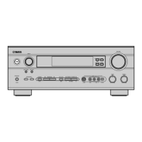
RX-V340 Front Panel

Illustration of the front panel controls and layout for RX-V340 (C, L, R, T models).

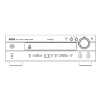
RX-V340RDS Front Panel

Illustration of the front panel controls and layout for RX-V340RDS (B, G models).

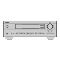
HTR-5630 Front Panel

Illustration of the front panel controls and layout for HTR-5630 (U, C, A, R, T, K models).

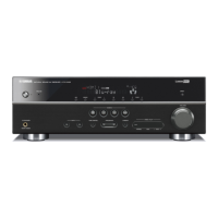
HTR-5630RDS Front Panel

Illustration of the front panel controls and layout for HTR-5630RDS (B, G models).

Rear Panel Connections

DSP-AX340 Rear Panel

Illustration of the rear panel connections for the DSP-AX340 (J model).

RX-V340 Rear Panel (C Model)

Illustration of the rear panel connections for the RX-V340 (C model).

RX-V340 Rear Panel (L Model)

Illustration of the rear panel connections for the RX-V340 (L model).

RX-V340 Rear Panel (R Model)

Illustration of the rear panel connections for the RX-V340 (R model).

RX-V340 Rear Panel (T Model)

RX-V340RDS Rear Panel

Illustration of the rear panel connections for the RX-V340RDS (B, G models).

HTR-5630 Rear Panel (U, C Models)

Illustration of the rear panel connections for the HTR-5630 (U, C models).

HTR-5630 Rear Panel (A Model)

Illustration of the rear panel connections for the HTR-5630 (A model).

HTR-5630 Rear Panel (L Model)

HTR-5630 Rear Panel (R Model)

Illustration of the rear panel connections for the HTR-5630 (R model).

HTR-5630 Rear Panel (T Model)

Illustration of the rear panel connections for the HTR-5630 (T model).

HTR-5630 Rear Panel (K Model)

Illustration of the rear panel connections for the HTR-5630 (K model).

HTR-5630RDS Rear Panel

DSP-AX340 Rear Panel

Illustration of the rear panel connections for the DSP-AX340 (J model).

Remote Control Layouts

Visual guide to remote control buttons.

RX-V340 Remote Control

Layout of buttons on the remote control for RX-V340 (C, L, R, T models).

HTR-5630 Remote Control

Layout of buttons on the remote control for HTR-5630 (U, C, A, L, R, T, K models).

DSP-AX340 Remote Control

Layout of buttons on the remote control for DSP-AX340 (J model).

RX-V340RDS Remote Control

Layout of buttons on the remote control for RX-V340RDS (B, G models).

HTR-5630RDS Remote Control

Layout of buttons on the remote control for HTR-5630RDS (B, G models).

Audio Section Specifications

Minimum RMS Output Power

Minimum RMS output power ratings for various channels and impedance conditions.

Maximum Power Output (EIAJ)

Maximum power output specifications based on EIAJ standards for different models.

DIN Standard Output Power

Output power ratings according to DIN standards for specific models and conditions.

Dynamic Power Output (IHF)

Dynamic power output measurements under IHF conditions for different impedance loads.

Tone Control Characteristics

Specifications for the bass and treble boost/cut ranges and frequency.

Filter Characteristics

Specifications for high-pass (HPF) and low-pass (LPF) filter characteristics.

Video Section Specifications

Specifications related to video signal types, levels, and frequency response.

FM/AM and General Specifications

AM Tuner Specifications

Tuning range and usable sensitivity specifications for the AM tuner section.

FM Tuner Specifications

Specifications for FM tuner: tuning range, sensitivity, selectivity, S/N ratio, and distortion.

General Unit Specifications

General specifications including power supply voltage, power consumption, dimensions, and weight.

Included Accessories

List of accessories provided with the product, such as remote control and antennas.

Set Menu Table

Basic Setup Menu Options

Configuration options for basic settings like Room Size, Speaker Setup, and LFE Level.

Sound Menu Options

Sound related settings including Speaker Set, Distance, LFE Level, and Tone Controls.

Input Assignment Options

Options for assigning input signals to specific terminals and input modes.

Option Menu Settings

Configuration options for display settings, memory guard, audio mute, and dual mono.

Parameter Variable Ranges

DSP Level Parameter Range

Variable range for the DSP Level parameter, including min, max, and step values.

5ch Stereo Parameter Ranges

Variable ranges for 5ch stereo parameters like CT Level, RL Level, and RR Level.

Pro Logic II Music Parameter Ranges

Variable ranges for Pro Logic II parameters like Panorama, Dimensions, and CT Width.

Internal View of Components

Main (2) PCB Identification

Identification and location of the Main (2) Printed Circuit Board within the unit.

Function (7) PCB Identification (R Model)

Identification and location of the Function (7) PCB, specific to R models.

Main (4) PCB Identification

Identification and location of the Main (4) Printed Circuit Board within the unit.

Tuner Module Identification

Identification and location of the Tuner module within the unit.

Main (3) PCB Identification

Identification and location of the Main (3) Printed Circuit Board within the unit.

Function (3) PCB Identification

Identification and location of the Function (3) Printed Circuit Board within the unit.

Function (6) PCB Identification

Identification and location of the Function (6) Printed Circuit Board within the unit.

Function (1) PCB Identification

Identification and location of the Function (1) Printed Circuit Board within the unit.

DSP PCB Identification

Identification and location of the DSP Printed Circuit Board within the unit.

Function (2) PCB Identification

Identification and location of the Function (2) Printed Circuit Board within the unit.

Main (1) PCB Identification

Identification and location of the Main (1) Printed Circuit Board within the unit.

Function (4) PCB Identification

Identification and location of the Function (4) Printed Circuit Board within the unit.

Function (8) PCB Identification

Identification and location of the Function (8) Printed Circuit Board within the unit.

Power Transformer Identification

Identification and location of the Power Transformer within the unit.

Main (5) PCB Identification

Identification and location of the Main (5) Printed Circuit Board within the unit.

Function (5) PCB Identification

Identification and location of the Function (5) Printed Circuit Board within the unit.

Disassembly Procedures Overview

Top Cover Removal

Instructions for removing the top cover, including screw locations and sliding direction.

Front Panel Unit Removal

Steps to remove the front panel unit, involving harness, screws, and sliding the unit forward.

DSP PCB Removal

Procedure for removing the DSP PCB with its support, including connector and screw details.

Main and Function PCB Removal

CB281 and CB471 Removal

Instructions to remove connectors CB281 and CB471 as part of PCB removal.

Screw Removal (16)

Instructions to remove 16 screws, identified by number ⑦, as part of the disassembly process.

Main/Function PCBs and Tuner Removal

Steps to remove MAIN (3), MAIN (4), FUNCTION (3), FUNCTION (6) PCBs, and the Tuner.

Main (1) and Function PCB Removal

CB303 and CB304 Connector Removal

Instructions to remove connectors CB303 and CB304 as part of the PCB removal process.

Screw Removal (2)

Instructions to remove 2 screws, identified by number ⑧, during disassembly.

Screw Removal (7)

Instructions to remove 7 screws, identified by number ⑨, during disassembly.

Main (1) and Function PCBs Removal

Steps to remove MAIN (1), FUNCTION (1), and FUNCTION (8) PCBs.

PCB Checking and Reassembly Notes

Reconnect Cables and Connectors

Instruction to reconnect all previously disconnected cables and connectors during PCB checks.

Flat Cable Polarity Caution

Caution to ensure correct polarity when connecting flat cables during PCB checks.

MAIN (1) PCB Grounding

Note on MAIN (1) PCB grounding issues and how to connect it to the chassis.

PCB Operation Independence

Information that FUNCTION and MAIN PCBs can operate even if the DSP PCB is removed.

Self Diagnosis (DIAG) Function

DSP THROUGH Diagnostic Menu

Diagnostic menu item for DSP through functions, including sub-menu options like Analog Bypass.

RAM THROUGH Diagnostic Menu

Diagnostic menu item for RAM through functions, covering YSS ODB and other settings.

PRO LOGIC / NEO6 Diagnostic Menu

Diagnostic menu for Pro Logic and Neo:6 settings, including applicable models.

Speaker Set Diagnostic Menu

Diagnostic menu for speaker settings, covering main, center, LFE, and front mix options.

Margin Check Diagnostic Menu

Diagnostic menu for margin check, covering main channel margins and tone control.

Other Input Diagnostic Menu

Diagnostic menu for other input settings, including external decoder.

Display Check Diagnostic Menu

Diagnostic menu for checking the VFD display modes and segments.

Manual Test Diagnostic Menu

Diagnostic menu for manual tests, allowing output of noise from specific channels.

Factory Preset Diagnostic Menu

Diagnostic menu for factory presets, related to memory initialization inhibition or reservation.

AD Data Check / Fan Test Diagnostic Menu

Diagnostic menu for AD data check and fan test, including DC/PS, THM/Fan values.

IF Status Diagnostic Menu

DSP RAM Check Diagnostic Menu

Diagnostic menu to check bus connection for YSS938 and external RAM.

SD DL CODE Diagnostic Menu

Diagnostic menu to display data version, TOC info, and sum calculated value for the second decoder.

Soft Switch Diagnostic Menu

Diagnostic menu to switch function settings on PCB via software for product activation.

ROM Version/Check Sum/Port Diagnostic Menu

Diagnostic menu to display microprocessor version, checksum, and port settings.

Starting the DIAG Function

DIAG Function Activation Procedure

Procedure to activate DIAG mode by pressing specific unit keys simultaneously with the STANDBY/ON key.

DIAG with Protection Canceled

Crucial for troubleshooting protection issues.

Canceling Protection for DIAG

Steps to cancel protection function to enable DIAG mode for diagnosis. Caution advised.

Caution During Protection Cancel Mode

Warning about potential damage to the unit when using DIAG mode with protection functions disabled.

Canceling the DIAG Function

How to exit DIAG mode.

DIAG Cancellation: Preset Setting

Procedure to set DIAG menu No.9 (Factory Preset) before canceling DIAG to preserve memory.

DIAG Cancellation: Power Off

Final step to cancel DIAG mode by turning off the unit's power using the STANDBY/ON key.

DIAG Mode Display Information

DIAG Display: No Protection History

How the FL display shows information when no protection history is present.

DIAG Display: Protection History Present

Interpreting the FL display when protection history data is shown, including causes.

DIAG Cause: Excessive Current

Explanation of excessive current as a cause for protection, with supplementary information on detection.

DIAG Cause: Abnormal Power Supply Voltage

Explanation of abnormal power supply voltage as a cause for protection, with display interpretation.

DIAG Cause: Abnormal DC Output

DIAG Cause: Excessive Heat Sink Temperature

Explanation of excessive heat sink temperature as a cause for protection.

Additional Protection Causes

Mention of other potential causes for protection activation, such as loose connections or CPU issues.

Protection History Storage and Clearing

Explanation of how protection history is stored, retained, and cleared.

DIAG Menu Operation Display

How the FL indicator shows the function currently in operation during DIAG.

DIAG Menu and Sub-Menu Operation

DIAG Menu Selection Method

Instructions on how to select DIAG menus using the PRESET/TUNING keys.

DIAG Sub-Menu Selection Method

Instructions on how to select sub-menus using the PROGRAM keys.

Functions Available During DIAG Mode

Features usable within DIAG.

DIAG Mode: Input Selection

Ability to change input selection and 6CH input settings while in DIAG mode.

DIAG Mode: Speaker Level Adjustment

Adjustment of center, rear, and subwoofer levels during DIAG mode.

DIAG Mode: Muting Function

Ability to use the muting function while in DIAG mode.

DIAG Mode: Power Control

Ability to turn the unit power on and off while in DIAG mode.

DIAG Mode: Master Volume Control

Ability to control the master volume while in DIAG mode.

Initial Settings for DIAG Mode

Default settings when entering DIAG.

DIAG Initial Setting: Master Volume

The initial setting for master volume when starting DIAG mode is -40dB.

DIAG Initial Setting: Input Source

The initial input source setting for DIAG mode is DVD with 6CH input OFF.

DIAG Initial Setting: Effect Level

The initial effect level setting for DIAG mode is 0dB.

DIAG Initial Setting: Audio Mute

The initial audio mute setting for DIAG mode is OFF.

DIAG Initial Setting: Speaker Configuration

The initial speaker setting for DIAG mode is LARGE/BASS OUT=BOTH.

DIAG Initial Setting: Menu Selection

The initial DIAG menu selected is DSP THROUGH (Analog Bypass).

DIAG Menu Details

DIAG Menu: Full-Bit Output Options

Explanation of full-bit output capability without head margin in certain DIAG modes.

DIAG Menu: DSP THROUGH Function

Details on selecting YSS938's Main DSP for MAIN L/R output in DSP THROUGH mode.

DIAG Menu: Analog Bypass Details

Explanation of how L/R signals are output directly without DSP processing in Analog Bypass.

DIAG Menu: YSS 0dB Signal Output

Details on YSS 0dB signal output, including head margin and SWFR signal addition.

DIAG Menu: YSS Front 0dB Signal Output

Explanation of YSS Front 0dB signal output, including head margin at main CH.

DIAG Menu: YSS FULL BIT Output

DIAG Menu: YSS FULL BIT F Output

Explanation of YSS FULL BIT F output for front CH signal at the main CH.

DIAG Menu: DSP THROUGH Block Diagram

Block diagram illustrating the DSP THROUGH signal path, including Analog and Digital inputs.

DIAG Menu: RAM THROUGH Function

DIAG Menu: PRO LOGIC Function

DIAG Menu: PRO LOGIC I Details

Details on PRO LOGIC I processing, including signal paths and output.

DIAG Menu: PRO LOGIC II Details

Details on PRO LOGIC II processing, including signal paths and output.

DIAG Menu: Neo:6 Function

DIAG Menu: Speaker Set Function

Details on automatic input signal switching and DSP output for Speaker Set function.

Speaker Set: LARGE Mode

Description of the LARGE speaker mode for high bass reproduction performance speakers.

Speaker Set: SMALL Mode

Description of the SMALL speaker mode for low bass reproduction performance speakers.

Speaker Set: NONE Mode

Description of the NONE speaker mode, used when no center speaker is present.

DIAG: DVD Analog Input Reference Data

DIAG Menu: Margin Check Function

Explanation of Margin Check function, outputting signal with head margin.

DIAG Menu: Main 12dB Margin

Details on the MAIN 12dB Margin setting within the Margin Check function.

DIAG Menu: Main 18dB Margin

Details on the MAIN 18dB Margin setting within the Margin Check function.

DIAG Menu: Other Input Function

DIAG Menu: Display Check Function

Program to check the FL display section, showing condition variations based on sub-menu operation.

Display Check: Initial Display

Description of the initial display mode for the FL display check.

Display Check: Lattice Lighting

Description of the lattice lighting mode for the FL display check.

Display Check: Short Detection

How to check for shorts between segments in the FL display.

DIAG Menu: Manual Test Function

Manual Test: All Channels Output

Manual test mode where noise is output from all channels.

Manual Test: Main R Channel Output

Manual test mode for outputting noise from the MAIN R channel.

Manual Test: Main L Channel Output

Manual test mode for outputting noise from the MAIN L channel.

Manual Test: Rear R Channel Output

Manual test mode for outputting noise from the REAR R channel.

Manual Test: Rear L Channel Output

Manual test mode for outputting noise from the REAR L channel.

Manual Test: LFE Channel Output

Manual test mode for outputting noise from the SUB WOOFER channel.

DIAG Menu: Factory Preset Function

Menu for reserving and inhibiting backup RAM initialization using EFFECT OFF.

Factory Preset: Prevent Initialization

Setting to prevent RAM initialization, protecting user-set values.

Factory Preset: Reserve Initialization

Setting to reserve RAM initialization for resetting to factory settings.

DIAG Menu: AD Data Check and Fan Test

AD Data Check: DC/PS Protection

Checks DC and Power Supply protection values, indicating normal ranges and function.

AD Data Check: THM/Fan Status

Checks temperature detection (THM) and fan drive level (Fan) values.

DIAG Menu: Impedance/Power Limit Check

DIAG Menu: Panel Key Check (K0/K1)

Checks panel keys for proper A/D function, referring to table for constants and solder conditions.

IF Status Function

IF Status: Internal Microprocessor Status

Indicates the status information of the microprocessor (IS1, IS2).

IF Status: Digital Input/Output Settings

Shows digital input/output setting value, REC OUT selection, and INPUT selection.

IF Status: Reproduction Signal Fs Info

Displays Fs information of the reproduction signal, including Analog and Digital modes.

IF Status: Audio Code Mode Info

Displays audio code mode information of the reproduction signal.

IF Status: Reproduction Signal Format Info

Displays format information of the reproduction signal, including analog/digital processing.

IF Status: Signal Processing Status

IF Status: Channel Status (IEC60958)

Indicates channel status information of the input signal according to IEC60958 standards.

IF Status: Dolby Digital Bit Stream Info

Indicates information of the bit stream within the Dolby Digital signal.

IF Status: DTS Bit Stream Info

Indicates information of the bit stream within the DTS signal.

IF Status: YSS938 Device Status

Indicates device status information of YSS938 (IC601).

DIAG Menu: DSP RAM Check Function

DSP RAM Check: YSS938 Bus Status

Displays the bus check status for YSS938, indicating if the bus is being checked or if errors are detected.

DSP RAM Check: PLD/SRAM Bus Status

Displays the bus check status for PLD/SRAM, indicating if the bus is being checked or if errors are detected.

DIAG Menu: SD DL CODE Function

Displays data version, TOC information, and sum calculated value for the second decoder.

DIAG Menu: Soft Switch Function

Soft Switch: SW Mode Selection

Allows selection between PCB mode or SOFT mode for SW mode.

Soft Switch: Model Setting

Allows selection of the unit model setting between V340 and V340T.

Soft Switch: Tuner Destination Setting

Allows selection of tuner destination among J, UC, ALG, or R.

Soft Switch: Tuner Existence Setting

Allows selection for tuner existence, either NOT or EXIST.

Soft Switch: RDS Existence Setting

Allows selection for RDS existence, either NOT or EXIST.

Soft Switch: Zone 2 Existence Setting

Allows selection for Zone 2 existence, either NOT or EXIST.

Soft Switch: Video Format Setting (J Model)

Allows selection of video format (NTSC or PAL), applicable to J models only.

DIAG Menu: Microprocessor Information

Microprocessor Info: Version

Displays version information: Release 1 digit, Main version 2 digit, DSP version 2 digit.

Microprocessor Info: Checksum

Displays checksum information for all program areas.

Microprocessor Info: Port Setting Check

Checks port settings to judge microprocessor function.

Microprocessor Info: AAC Function Port State

Displays the state of the AAC function detection port.

Idling Current Confirmation

Main (1) PCB Idling Current Check

Procedure to confirm idling current voltage across terminals R359 to R361 on Main (1) PCB.

Idling Current Check: Pre-Check Preparation

Preparation steps before confirmation: remove FUNCTION (4) PCB and connect G651 to chassis.

Display Data Information

Display Data: V581 Model Information

Information regarding display model V581: HNA-16MM43 (WA531200).

Pin Connection Diagrams

Diagrams showing pin connections for various ICs and components.

Grid Assignment Diagrams

Diagrams illustrating grid assignments for various input and output signals.

Anode Connection Pinouts

IC Data: M3062VMGP Microcontroller

M3062VMGP Microcontroller Pinout

Pinout and function details for the M3062VMGP microcontroller (Main CPU).

M3062VMGP Microcontroller Pinout Details

IC803 YSS938 DSP Chip Details

YSS938 Pin: SELOA

Function of the SELOA pin on the YSS938 chip.

YSS938 Pin: SELOB

Function of the SELOB pin on the YSS938 chip.

YSS938 Pin: SDWCKI1

Function of the SDWCKI1 pin on the YSS938 chip.

YSS938 Pin: SDBCKI1

Function of the SDBCKI1 pin on the YSS938 chip.

YSS938 Pin: XO

YSS938 Pin: XI

Function of the XI pin on the YSS938 chip.

YSS938 Pin: SELI1

Function of the SELI1 pin on the YSS938 chip.

YSS938 Pin: SELIO

Function of the SELIO pin on the YSS938 chip.

YSS938 Pin: SELOA

Function of the SELOA pin on the YSS938 chip.

YSS938 Pin: SELOB

Function of the SELOB pin on the YSS938 chip.

YSS938 Pin: SDWCKI1

YSS938 Pin: SDBCKI1

Function of the SDBCKI1 pin on the YSS938 chip.

YSS938 Pin: VSS

Function of the VSS pin on the YSS938 chip.

YSS938 Pin: SDOB3

Function of the SDOB3 pin on the YSS938 chip.

YSS938 Pin: SDOB2

Function of the SDOB2 pin on the YSS938 chip.

YSS938 Pin: RAMA5

YSS938 Pin: RAMA2

Function of the RAMA2 pin on the YSS938 chip.

YSS938 Pin: SELI13

Function of the SELI13 pin on the YSS938 chip.

YSS938 Pin: SELI12

Function of the SELI12 pin on the YSS938 chip.

YSS938 Pin: SELI11

Function of the SELI11 pin on the YSS938 chip.

YSS938 Pin: SELI10

Function of the SELI10 pin on the YSS938 chip.

YSS938 Pin: SELI9

Function of the SELI9 pin on the YSS938 chip.

YSS938 Pin: RAMA4

Function of the RAMA4 pin on the YSS938 chip.

System Block Diagram

Main Signal Paths Block Diagram

Block diagram illustrating the main signal flow through the unit.

DSP Signal Path Block Diagram

Block diagram showing the signal path through the DSP section.

Function Block Diagram

Block diagram illustrating the signal paths related to various functions.

Printed Circuit Board Layout (DSP PCB)

DSP PCB Component Layout (Lead Type)

Component layout diagram for the DSP PCB (Lead Type Device).

DSP PCB Component Layout (Surface Mount)

Component layout diagram for the DSP PCB (Surface Mount Device).

Semiconductor Component Locations

Table mapping semiconductor reference numbers to their locations on the PCB.

Printed Circuit Board Layout (Function PCBs)

Function (2) PCB Layout (Lead Type)

Component layout diagram for the Function (2) PCB (Lead Type Device).

Main (1) PCB Component Layout

Component layout diagram for the Main (1) PCB.

Function (4) PCB Layout (Lead Type)

Component layout diagram for the Function (4) PCB (Lead Type Device).

Power Transformer Location

Location of the power transformer on the printed circuit board.

Function (5) PCB Layout (Lead Type)

Component layout diagram for the Function (5) PCB (Lead Type Device).

Semiconductor Component Locations (Function 2 PCB)

Mapping of semiconductors to locations on the Function (2) PCB.

Printed Circuit Board Layout (Function 2 & 3 PCBs)

Function (2) PCB Layout (Surface Mount)

Component layout diagram for the Function (2) PCB (Surface Mount Device).

Function (3) PCB Layout (Surface Mount)

Component layout diagram for the Function (3) PCB (Surface Mount Device).

Semiconductor Component Locations (Function 2 & 3 PCBs)

Mapping of semiconductors to locations on Function (2) and (3) PCBs.

Printed Circuit Board Layout (Function 1, 6, 7, 8 PCBs)

Function (7) PCB Layout (Lead Type)

Component layout diagram for the Function (7) PCB (Lead Type Device).

Function (3) PCB Layout (Lead Type)

Component layout diagram for the Function (3) PCB (Lead Type Device).

Function (8) PCB Layout (Lead Type)

Component layout diagram for the Function (8) PCB (Lead Type Device).

Function (1) PCB Layout (Lead Type)

Component layout diagram for the Function (1) PCB (Lead Type Device).

DSP PCB Layout (Lead Type)

Component layout diagram for the DSP PCB (Lead Type Device).

Function (6) PCB Layout (Lead Type)

Component layout diagram for the Function (6) PCB (Lead Type Device).

Semiconductor Component Locations (Function 1, 6, 7, 8 PCBs)

Mapping of semiconductors to locations on Function (1, 6, 7, 8) PCBs.

Printed Circuit Board Layout (MAIN PCBs)

MAIN (2) PCB Layout (Surface Mount)

Component layout diagram for the MAIN (2) PCB (Surface Mount Device).

MAIN (3) PCB Layout (Surface Mount)

Component layout diagram for the MAIN (3) PCB (Surface Mount Device).

MAIN (5) PCB Layout (Surface Mount)

Component layout diagram for the MAIN (5) PCB (Surface Mount Device).

Printed Circuit Board Layout (MAIN PCB)

MAIN (1) PCB Layout (Surface Mount)

Component layout diagram for the MAIN (1) PCB (Surface Mount Device).

Semiconductor Component Locations (MAIN 1 PCB)

Mapping of semiconductors to locations on the MAIN (1) PCB.

Printed Circuit Board Layout (MAIN 1 PCB)

Semiconductor Component Locations (MAIN 1 PCB)

Mapping of semiconductors to locations on the MAIN (1) PCB.

Printed Circuit Board Layout (MAIN 2, 3, 4, 5 PCBs)

MAIN (2) PCB Layout (Surface Mount)

Component layout diagram for the MAIN (2) PCB (Surface Mount Device).

MAIN (3) PCB Layout (Surface Mount)

Component layout diagram for the MAIN (3) PCB (Surface Mount Device).

MAIN (5) PCB Layout (Surface Mount)

Component layout diagram for the MAIN (5) PCB (Surface Mount Device).

MAIN (4) PCB Layout (Lead Type Device)

Component layout diagram for the MAIN (4) PCB (Lead Type Device).

Semiconductor Component Locations (MAIN 2, 3, 4, 5 PCBs)

Mapping of semiconductors to locations on MAIN (2, 3, 4, 5) PCBs.

Printed Circuit Board Layout (MAIN 2, 3, 5 PCBs)

MAIN (2) PCB Layout (Surface Mount)

Component layout diagram for the MAIN (2) PCB (Surface Mount Device).

MAIN (3) PCB Layout (Surface Mount)

Component layout diagram for the MAIN (3) PCB (Surface Mount Device).

MAIN (5) PCB Layout (Surface Mount)

Component layout diagram for the MAIN (5) PCB (Surface Mount Device).

Semiconductor Component Locations (MAIN 2, 3, 5 PCBs)

Mapping of semiconductors to locations on MAIN (2, 3, 5) PCBs.

Pin Connection Diagrams

ICs Pin Connection Diagrams

Pinout diagrams for various integrated circuits (ICs).

Diodes Pin Connection Diagrams

Pinout diagrams for various diodes.

Transistors Pin Connection Diagrams

Pinout diagrams for various transistors.

Schematic Diagram (Main 1/2)

Main Signal Paths Schematic

Schematic diagram illustrating main signal paths and component interconnections.

Micro Computer Schematic

Schematic diagram detailing the microcomputer circuit.

Power Relay and Control Schematic

Schematic detailing power relay and control circuits.

Schematic Diagram (Main 2/2)

Input Selector Schematic

Schematic diagram for the input selector circuit.

Level Shift Circuit Schematic

Schematic diagram for the level shift circuit.

Power Detector Schematic

Schematic diagram for the power detector circuit.

Electrical Parts List

Component Abbreviations

List of abbreviations used for component types in the parts list.

P.C.B. DSP Parts List

DSP PCB Part Numbers (Capacitors)

List of capacitors (C) used on the DSP PCB, with part numbers and specifications.

DSP PCB Part Numbers (Diodes)

List of diodes (D) used on the DSP PCB, with part numbers and specifications.

DSP PCB Parts List (Capacitors)

DSP PCB Part Numbers (Capacitors C850-C903)

List of capacitors (C850-C903) on the DSP PCB, with part numbers and specifications.

DSP PCB Parts List (Capacitors C904-C948)

DSP PCB Part Numbers (Capacitors C904-C948)

List of capacitors (C904-C948) on the DSP PCB, with part numbers and specifications.

DSP PCB Part Numbers (Diodes D801-D808)

List of diodes (D801-D808) on the DSP PCB, with part numbers and specifications.

DSP PCB Parts List (Diodes D809-D477)

DSP PCB Part Numbers (Diodes D809-D477)

List of diodes (D809-D477) on the DSP PCB, with part numbers and specifications.

P.C.B. FUNCTION Parts List (Capacitors C101-C343)

P.C.B. FUNCTION Parts List (Capacitors C101-C343)

List of capacitors (C101-C343) on the P.C.B. FUNCTION, with part numbers.

P.C.B. FUNCTION Parts List (Capacitors C344-C513)

P.C.B. FUNCTION Parts List (Capacitors C344-C513)

List of capacitors (C344-C513) on the P.C.B. FUNCTION, with part numbers.

P.C.B. FUNCTION Parts List (Capacitors C510-C666)

P.C.B. FUNCTION Parts List (Capacitors C510-C666)

List of capacitors (C510-C666) on the P.C.B. FUNCTION, with part numbers.

P.C.B. FUNCTION Parts List (Capacitors C668-C775)

P.C.B. FUNCTION Parts List (Capacitors C668-C775)

List of capacitors (C668-C775) on the P.C.B. FUNCTION, with part numbers.

P.C.B. MAIN Parts List (Capacitors C282-C343)

P.C.B. MAIN Parts List (Capacitors C282-C343)

List of capacitors (C282-C343) on the P.C.B. MAIN, with part numbers.

P.C.B. MAIN Parts List (Capacitors C344-C513)

P.C.B. MAIN Parts List (Capacitors C344-C513)

List of capacitors (C344-C513) on the P.C.B. MAIN, with part numbers.

P.C.B. MAIN Parts List (Capacitors C510-C513)

P.C.B. MAIN Parts List (Capacitors C510-C513)

List of capacitors (C510-C513) on the P.C.B. MAIN, with part numbers.

P.C.B. MAIN Parts List (Capacitors C651-C775)

P.C.B. MAIN Parts List (Capacitors C651-C775)

List of capacitors (C651-C775) on the P.C.B. MAIN, with part numbers.

P.C.B. MAIN Parts List (Capacitors C771-C775)

P.C.B. MAIN Parts List (Capacitors C771-C775)

List of capacitors (C771-C775) on the P.C.B. MAIN, with part numbers.

P.C.B. MAIN Parts List (Resistors R307-R383)

P.C.B. MAIN Parts List (Resistors R307-R383)

List of resistors (R307-R383) on the P.C.B. MAIN, with part numbers.

Chip Resistors List

Chip Resistors (R350-R359100)

List of chip resistors (R350-R359100) with resistance values and part numbers.

Parts List for Carbon Resistors

Carbon Resistor Part Numbers (1.0 Ohm - 9.1 Kilo Ohm)

Part numbers for carbon resistors from 1.0 Ohm to 9.1 Kilo Ohm.

Carbon Resistor Part Numbers (10 Kilo Ohm - 4.7 Mega Ohm)

Part numbers for carbon resistors from 10 Kilo Ohm to 4.7 Mega Ohm.

Exploded View

Exploded View: R Model Components

Exploded view illustrating components for R models.

Exploded View: J, U, C, R, T, K, A, L Model Components

Exploded view illustrating components for J, U, C, R, T, K, A, L models.

Exploded View: B, G Model Components

Exploded view illustrating components for B, G models.

Mechanical Parts List

Mechanical Parts: Front Panels and Covers

List of mechanical parts including front panels, top covers, and rear panels.

Mechanical Parts: Buttons and Cables

List of mechanical parts including button cases, escutcheons, and flexible flat cables.

Mechanical Parts: Legs and Knobs

List of mechanical parts including legs, knobs, and PCB supports.

Mechanical Parts: Screws and Ties

List of mechanical parts including screws, ties, and dampers.

Mechanical Parts: Tuners and Transformers

List of mechanical parts including tuners and power transformers.

Accessories List

List of included accessories like remote controls, antennas, and batteries.

Remote Control Schematic Diagram (RAV300)

Remote Control Key Codes (RAV300)

Table of key functions, codes, and data codes for the RAV300 remote control.

Remote Control Schematic Diagram (RAV16)

Remote Control Key Codes (RAV16)

Table of key functions, codes, and data codes for the RAV16 remote control.

Related product manuals