Do you have a question about the Yamaha HTR-5650 and is the answer not in the manual?
Verifies insulation of exposed surfaces from supply circuits for 120V models.
Warns about lead in solder and other chemicals, advising safe handling.
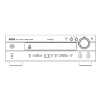
Front panel layout for RX-V540 and related models.
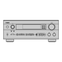
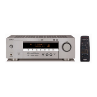
Front panel layout for HTR-5650 and related models.
Front panel layout for DSP-AX540 (J) model.
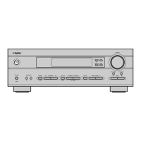
Front panel layout for RX-V440 and related models.
Rear panel layout for RX-V540 models.
Rear panel layout for RX-V540RDS models.
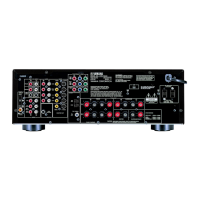
Rear panel layout for HTR-5650 models.
Rear panel layout for DSP-AX540 (J) model.
Rear panel layout for RX-V440 and related models.
Rear panel layout for HTR-5640 and related models.
Rear panel layout for HTR-5640RDS models.
Rear panel layout for DSP-AX440 (J) model.
Remote control layouts for specified models.
Remote control layouts for specified models.
Remote control layouts for specified models.
Remote control layouts for specified models.
Details audio output power, frequency response, and signal-to-noise ratio specifications.
Details video signal types, levels, and format specifications.
Lists frequency response for various monitor outputs.
Details FM tuner specifications like tuning range, sensitivity, and selectivity.
Details AM tuner specifications like tuning range and sensitivity.
Covers power supply, consumption, dimensions, weight, and available finishes.
Settings for room, subwoofer, and speaker configuration.
Adjustments for speaker level for each channel.
Speaker settings for size, rear, center, and bass.
Settings for speaker distance and effective distance.
Adjustments for subwoofer LFE level.
Settings for dynamic range control.
Settings for center channel equalization.
Controls for treble and bass tone.
Assignment of input/output terminals.
Selection of input mode.
Display settings for brightness.
Setting for memory guard.
Audio mute settings.
Zone settings.
Dual mono setting for J model.
Instructions for removing the top cover of the unit.
Instructions for removing the front panel unit and its connections.
Steps for removing the DSP printed circuit board.
Procedures for removing function PCBs and the tuner.
Steps for removing main and power PCBs.
Controls DSP signal routing for main L/R output, selecting YSS938 or analog bypass.
Function for YSS938, outputting CT signal via Sub DSP-DRAM.
Settings for Pro Logic and Neo:6 audio processing modes.
Speaker settings for size, rear, center, and bass.
Checks signal output including head margin with different dB margins.
Specifies external decoder input.
Checks FL display segments, dimming, and pattern.
DSP noise generator outputs test noise to specified channels.
Used to reserve and inhibit RAM initialization for factory settings.
Displays A/D conversion values for panel keys and protection functions.
Displays input function status and signal processing status in hexadecimal.
Self-diagnoses bus connection for YSS938 and external RAM.
Displays data version of FLASH ROM, TOC information, and sum calculated value.
Switches function settings on PCB via software for product activation.
Instructions to start diagnostic mode by pressing specific keys simultaneously with power.
How to enter DIAG mode with protection functions disabled.
Procedures for canceling DIAG mode and resetting settings.
Shows FL display of protection history, version, and DIAG menu.
Message displayed when no protection function history is found.
History display for protection due to abnormal DC output.
History display for protection due to excessive heat sink temperature.
Indicates function status on FL display during DIAG operation.
Stores and displays past protection function events.
Lists functions available during DIAG mode, excluding tuner and menu.
Details the initial settings applied when starting DIAG.
Explains how to navigate DIAG menus and sub-menus using main unit keys.
Explains full-bit output without head margin in specific modes.
Selects Main DSP of YSS938 for MAIN L/R output; ANALOG BYPASS passes signal directly.
Outputs signal including head margin.
Front CH signal with head margin output at main CH.
Outputs signal in digital full bit without head margin; SWFR signal not in full bit.
Front CH signal outputs in digital full bit at main CH.
Function for YSS938, outputting CT signal via Sub DSP-DRAM.
Details Pro Logic processing for L/C/R/RL/RR signals and output.
Details Pro Logic II processing and output options.
Describes Neo:6 processing by CS49329 and output through Sub DSP-DRAM.
Automatically identifies and switches input signals based on priority.
Signal output including head margin, with 12dB and 18dB margin checks.
Outputs signal input through 6CH INPUT terminals.
Programs to check FL display conditions like segments and dimming.
DSP noise generator outputs test noise to specified channels.
Reserves and inhibits backup RAM initialization.
Displays A/D conversion values of terminals for panel keys and protection functions.
Displays DC protection and power supply voltage protection values.
Displays temperature detection and fan drive level.
Detects impedance/power limiter settings and controls port output.
Checks panel key A/D function and confirms constants.
Displays input function status and signal processing status in hexadecimal.
Self-diagnoses bus connection for YSS938 and external RAM.
Displays data version of FLASH ROM, TOC information, and sum calculated value.
Switches function settings on PCB via software for product activation.
Displays version, checksum, and microprocessor port settings.
Confirms idling current by measuring voltage across terminals on the main PCB.
Shows pin assignments for various ICs and components.
Maps terminal connections to grid assignments.
Shows the anode connection details for various grid assignments.
Details the functions and I/O of the main CPU IC.
Shows the foil side layout of the DSP PCB with lead type devices.
Shows the foil side layout of the DSP PCB with surface mount devices.
Foil layout of the FUNCTION PCBs (Lead Type).
Foil layout of the OPERATION PCBs (Lead Type).
Foil layout of the MAIN PCBs (Lead Type).
Foil layout of the MAIN PCBs (Lead Type).
Foil layout of the FUNCTION PCBs (Surface Mount).
Foil layout of the OPERATION PCBs (Lead Type).
Foil layout of the OPERATION PCB (Surface Mount).
Foil layout of the OPERATION PCBs (Lead Type).
Foil layout of the OPERATION PCBs (Surface Mount).
Foil layout of the POWER PCBs (Lead Type).
Foil layout of the POWER PCBs (Lead Type) for RX-V440 models.
Foil layout of the VIDEO PCB (Lead Type).
Foil layout of the VIDEO PCB (Surface Mount).
Foil layout of the FUNCTION PCBs (Lead Type).
Foil layout of the FUNCTION PCBs (Surface Mount).
Pin connection diagrams for various integrated circuits.
Pin configurations and types of diodes used.
Pin configurations and types of transistors used.
Shows the foil side layout of the DSP PCB with lead type devices.
Shows the foil side layout of the DSP PCB with surface mount devices.
Foil layout of the FUNCTION PCBs (Lead Type).
Foil layout of the OPERATION PCBs (Lead Type).
Foil layout of the MAIN PCBs (Lead Type).
Foil layout of the MAIN PCBs (Lead Type).
Foil layout of the FUNCTION PCBs (Surface Mount).
Foil layout of the OPERATION PCBs (Lead Type).
Foil layout of the OPERATION PCB (Surface Mount).
Foil layout of the OPERATION PCBs (Lead Type).
Foil layout of the OPERATION PCBs (Surface Mount).
Foil layout of the POWER PCBs (Lead Type).
Foil layout of the POWER PCBs (Lead Type) for RX-V440 models.
Foil layout of the VIDEO PCB (Lead Type).
Foil layout of the VIDEO PCB (Surface Mount).
Foil layout of the FUNCTION PCBs (Lead Type).
Foil layout of the FUNCTION PCBs (Surface Mount).
Lists electrical components with their abbreviations and descriptions.
Lists parts for the DSP PCB.
Lists parts for the main PCB.
Lists parts for the DSP PCB.
Lists parts for the operation PCBs.
Lists parts for the power PCBs.
Lists parts for power and video PCBs.
Lists parts for the main PCBs.
Lists parts for the operation PCBs.
Lists parts for operation and video PCBs.
Lists parts for the main PCBs.
Lists parts for the main PCBs.
Lists parts for the main PCBs.
Lists parts for the main PCBs.
Lists parts for the power PCBs.
Lists parts for the power PCBs.
Lists parts for the power PCBs.
Lists parts for the power PCBs.
Lists parts for the power PCBs.
Lists parts for the power PCBs.
Lists parts for the power PCBs.
Lists parts for the power PCBs.
Lists parts for the power PCBs.
Lists parts for the power PCBs.
Lists parts for the power PCBs.
Lists various chip resistors with their part numbers and specifications.
Lists carbon resistors by value and part number.
Exploded view diagram showing component placement and numbers.