Do you have a question about the Yamaha HTR-6190 and is the answer not in the manual?
Table of contents listing all major sections and their corresponding page numbers.
Basic service procedures and safety precautions for authorized personnel.
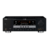
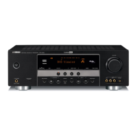
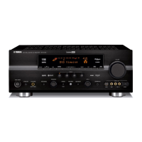
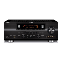
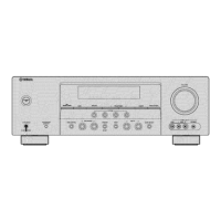
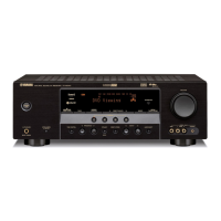
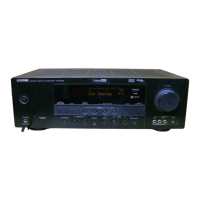
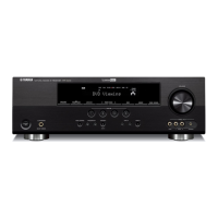
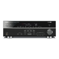
Diagrams showing front panel layouts for various models.
Diagrams showing rear panel connectors and labels for different models.
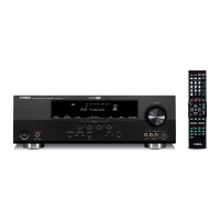
Images and descriptions of the remote controls provided with the unit.
Detailed technical specifications for audio and video sections of the unit.
Diagram showing the general internal layout of components within the unit.
Step-by-step instructions for safely disassembling the unit.
Procedures for updating the unit's firmware via CD, PC, or user mode.
Comprehensive menu for checking unit functions, status, and error codes.
Procedures for adjusting amplifier idling current.
Information on display patterns, pin connections, and grid assignments.
Detailed information on key integrated circuits, including pinouts.
High-level functional block diagrams of the unit's systems.
Component layout diagrams for various PCBs within the unit.
Diagrams showing pin connections for key components like ICs and transistors.
Detailed circuit diagrams for major functional blocks of the unit.
Comprehensive list of replaceable parts with part numbers and descriptions.
Diagrams and key code mapping for the remote controls.
Performance specifications for the audio amplifier section.
Specifications for video processing, inputs, and outputs.
Steps to update firmware using a DVD/CD player.
Steps to update firmware using a PC and serial cable.
Steps to update firmware via the user mode.
Procedure to enter the self-diagnostic mode.
Steps to exit the diagnostic mode and restore settings.
Procedure to bypass protection for diagnostic purposes.
Explanation of specific diagnostic menu items like DSP THROUGH.
Checking temperature sensor readings.
Checking amplifier output level monitoring.
Checking limiter control values.
Checking amplifier relay status.
Displaying the unit's model information.
Checking the functionality of front panel buttons.
Displaying input function status data.
Displaying the product ID stored in the HDMI module.
Displaying the vendor name stored in the HDMI module.
Block diagram for HDMI signal decoding.
Information on HDMI YGV signal processing.
Block diagram for HDMI signal input processing.
Details of digital component video processing.
Details of digital composite video processing.
Details of digital S-Video and Y/C signal processing.
Details of digital signal bypass through the unit.
Details of analog signal bypass through the unit.
Procedure for displaying test patterns for video output.
Displaying information about the input video signal.
Selecting the operational mode for PCB functions.
Setting the video format for NTSC or PAL.
Setting AAC audio stream availability.
Setting CSII audio stream availability.
Setting RDS data reception.
Setting XM service availability.
Setting Neural Surround audio processing.
Selecting FM/AM tuning modes.
Testing tuner functions for specific models.
Prevents user memory from being erased during factory reset.
Schedules factory reset upon next power-on.
Table of preset FM/AM station data.
Steps to measure and adjust amplifier idling current.
Detailed pinout diagrams for various components.
Diagram showing grid assignments for display elements.
Pinout and functions of the D-VIDEO microprocessor.
Functional block diagram of the audio signal path.
Block diagram illustrating the video signal path.
Block diagram of the unit's control and power systems.
Component layout for the DSP PCB (Side A).
Component layout for the DSP PCB (Side B).
Component layout for the FUNCTION (1) PCB (Side A).
Component layout for the FUNCTION (2) PCB (Side A).
Component layout for the FUNCTION (1) PCB (Side B).
Component layout for the FUNCTION (2) PCB (Side A).
Component layout for the FUNCTION (2) PCB (Side B).
Component layout for the OPERATION (1) PCB (Side A).
Component layout for the OPERATION (2) PCB (Side A).
Component layout for the OPERATION (1) PCB (Side B).
Component layout for the OPERATION (2) PCB (Side B).
Component layout for the OPERATION (3) PCB (Side A).
Component layout for the OPERATION (4) PCB (Side A).
Component layout for the OPERATION (5) PCB (Side A).
Component layout for the MAIN (1) PCB (Side A).
Component layout for the MAIN (1) PCB (Side B).
Component layout for the MAIN (2) PCB (Side A).
Component layout for the MAIN (3) PCB (Side A).
Component layout for the MAIN (4) PCB (Side A).
Component layout for the POWER (1) PCB (Side A).
Component layout for the POWER (1) PCB (Side B).
Component layout for the POWER (2) PCB (Side A).
Component layout for the POWER (5) PCB (Side A).
Component layout for the POWER (6) PCB (Side A).
Component layout for the POWER (5) PCB (Side B).
Component layout for the POWER (3) PCB (Side A).
Component layout for the POWER (3) PCB (Side B).
Component layout for the POWER (4) PCB (Side A).
Component layout for the POWER (4) PCB (Side B).
Component layout for the A-VIDEO PCB (Side A).
Component layout for the A-VIDEO PCB (Side B).
Component layout for the D-VIDEO PCB (Side A).
Component layout for the D-VIDEO PCB (Side B).
Component layout for the FL (1) PCB (Side A).
Component layout for the FL (1) PCB (Side B).
Component layout for the FL (2) PCB (Side A).
Component layout for the FL (2) PCB (Side B).
Component layout for the FL (3) PCB (Side A).
Component layout for the FL (4) PCB (Side A).
Component layout for the FL (3) PCB (Side B).
Component layout for the FL (4) PCB (Side B).
Component layout for the FL (5) PCB (Side A).
Component layout for the FL (6) PCB (Side A).
Component layout for the FL (5) PCB (Side B).
Component layout for the FL (6) PCB (Side B).
Functional block diagram of the audio signal path.
Schematic diagram section for DSP processing.
Schematic diagram section for DSP processing.
Schematic diagram section for DSP processing.
Continuation of the FUNCTION schematic diagram.
Continuation of the FUNCTION schematic diagram.
Continuation of the A-VIDEO schematic diagram.
Continuation of the D-VIDEO schematic diagram.
Continuation of the D-VIDEO schematic diagram.
Continuation of the D-VIDEO schematic diagram.
Continuation of the FL driver schematic diagram.
Explanation of abbreviations used in the replacement parts list.
Component list for the DSP Printed Circuit Board.
Continuation of the DSP PCB component list.
Continuation of the DSP PCB component list.
Component list for the FUNCTION Printed Circuit Board.
Continuation of the FUNCTION PCB component list.
Continuation of the FUNCTION PCB component list.
Continuation of the FUNCTION PCB component list.
Continuation of the FUNCTION PCB component list.
Component list for the POWER Printed Circuit Board.
Continuation of the POWER PCB component list.
Continuation of the POWER PCB component list.
Continuation of the POWER PCB component list.
Continuation of the POWER PCB component list.
Component lists for POWER and A-VIDEO PCBs.
Continuation of component lists for POWER and A-VIDEO PCBs.
Continuation of component lists for POWER and A-VIDEO PCBs.
Component list for the A-VIDEO Printed Circuit Board.
Continuation of the A-VIDEO PCB component list.
Continuation of the A-VIDEO PCB component list.
Component list for the D-VIDEO Printed Circuit Board.
Continuation of the D-VIDEO PCB component list.
Continuation of the D-VIDEO PCB component list.
Component list for the FL Printed Circuit Board.
Exploded view and parts list for the front panel and sub chassis.
Images of the remote control panels.
Continuation of remote control panel images.
Continuation of instructions for advanced setup options.
Continuation of instructions for advanced setup options.
| Channels | 7.1 |
|---|---|
| Frequency Response | 10 Hz-100 kHz (+0 dB, -3 dB) |
| Weight | 28.7 lbs (13 kg) |
| Signal-To-Noise Ratio | 100 dB |
| Input Impedance | 47 kΩ |
| Input Sensitivity | 200 mV |
| Audio D/A Converter | 192 kHz/24-bit |
| Surround System Class | 7.1 channel |
| HD Radio Ready | Yes |
| Digital Sound Processor (DSP) | Yes |
| DSP Preset Qty | 17 |
| Tuner Bands | AM/FM |
| Preset Station Qty | 40 |
| Power Supply | AC 120V, 60Hz |
| Response Bandwidth | 10 Hz - 100 kHz |
| Inputs | HDMI, Component video input, Composite video input, Digital audio input (optical), Digital audio input (coaxial) |
| Outputs | HDMI, Composite |
| Audio Formats Supported | Dolby Digital Plus, Dolby TrueHD, DTS-HD Master Audio |
| Video Formats Supported | 1080p |
| Dimensions | 17.1 x 6.8 x 17.1 inches (435 x 173 x 435 mm) |
| Additional Features | YPAO |
| Connectivity | HDMI, composite, component, digital audio (optical/coaxial), analog audio, speaker terminals |
| Speaker Impedance | 8 Ohm |
| FM Sensitivity | 1.0 μV |
| Power Consumption | 490 W |
| Dimensions (W x H x D) | 17.1 x 6.8 x 17.1 inches (435 x 173 x 435 mm) |