ABCDEFGH
1
2
3
4
5
6
IJKL
7
8
RX-E400
20
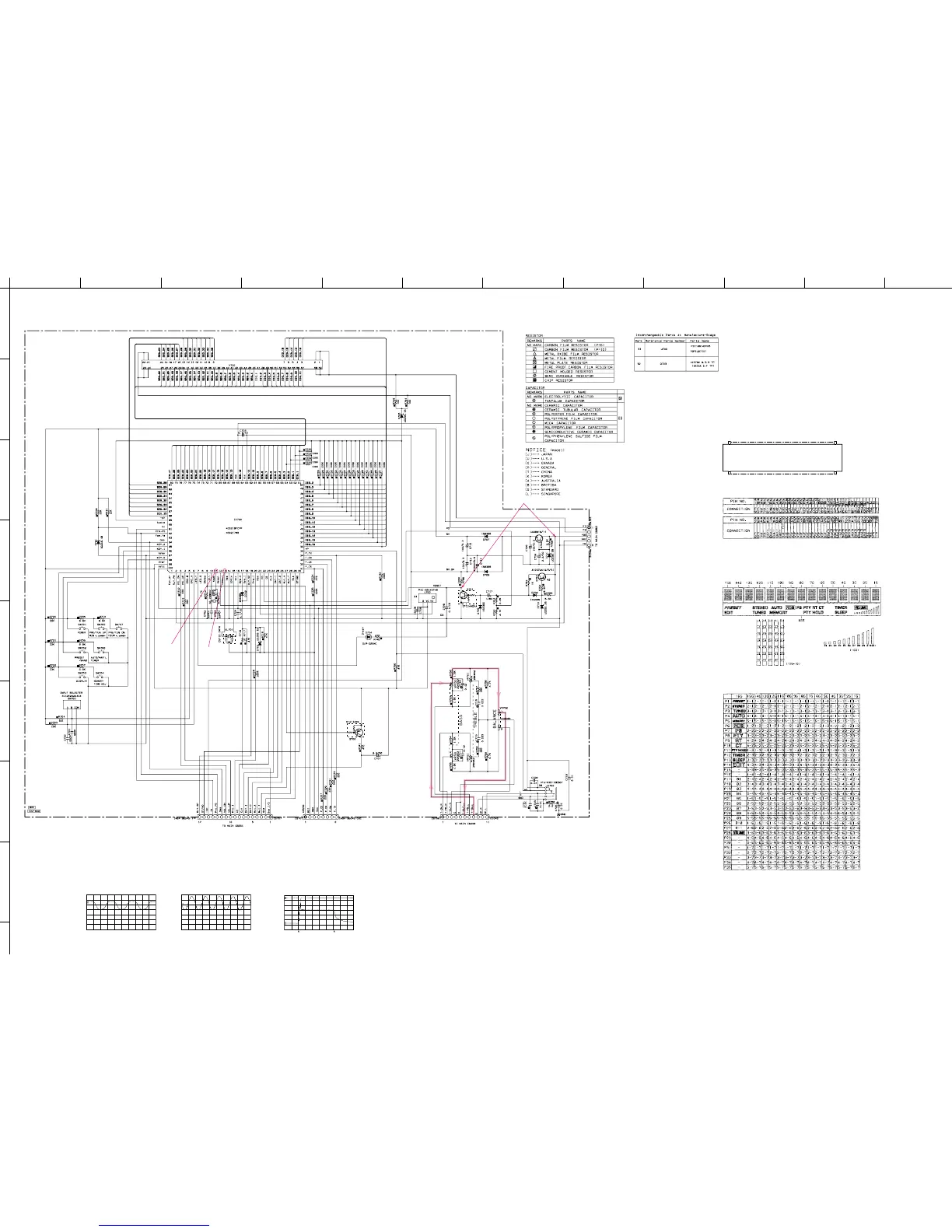
■ SCHEMATIC DIAGRAM (OPERATION)
* All voltage are measured with a 10MΩ/V DC electric volt meter.
* Components having special characteristics are marked Z and
must be replaced with parts having specifications equal to those
originally installed.
* Schematic diagram is subject to change without notice.
CPU
RESET
REGULATOR
-28.8
-28.8
-26.6
-24.5
-28.8
-28.8
-26.6
-26.6
-26.6
-24.5
-24.5
-26.7
-26.7
-26.7
-26.7
-26.7
-26.7
-23.9
-23.9
-24.1
-29.1
4.9 5.5
4.8 5.5
5.5
6.1
11.9
6.1
0
11.9
7.3
4.7
0
4.9
4.9
0
0
0
0
6.7
0
11.9
11.2
-28.8
-28.8
-26.7
-26.7
-26.7
-26.7
-26.7
-26.7
-26.7
-26.7
-28.8
-24.5
-26.6
-28.8
-28.8
-28.8
-24.6
-26.6
-28.9
-28.9
-28.9
-24.6
-26.6
-28.9
-28.9
0
-28.9
4.8
-24.6
-26.7
-26.7
-28.9
-28.9
-24.6
-28.9
-26.7
-24.5
-24.5
-26.7
-26.7
4.7
0
0
4.9
4.9
0
0
0
1.1
1.6
4.7
2.3
0
2.1
4.8
0
0
0
0
4.7
0
4.9
4.9
0
4.8
0.1
0
4.7
4.7
3.8
4.8
-26.7
-26.7
-26.7
-26.7
-26.7
-26.7
-26.7
0
0
0
0
0
-28.8
-26.6
-26.6
-26.6
-24.5
-24.5
-26.7
-28.8
-29.1
2.5
0
0
4.9
4.9
0
4.7
4.9
0
0
2.7
2.5
1.8
4.9
4.9
0
4.9
4.9
4.9
-24.6
-24.6
-26.6
-28.9
-28.9
-28.9
-24.6
-24.5
-24.5
-26.6
-28.9
-28.9
-28.9
-28.9
-28.9
-28.9
-24.6
-26.7
-26.7
-26.7
-26.7
-26.7
-26.7
-26.7
-26.7
-26.7
-26.7
-26.7
-26.7
-26.7
-26.7
-26.7
w
q
e
P-19 [E-3]
P-19 [F-3]
P-19 [F-3]
CH 2
CH 1
Point q (Pin 11 of IC700)
V : 2V/div, H : 10µsec/div
DC, 1 : 1 probe
0V
Point e
CH 1 : Collector of Q701
CH 2 : Collector of Q702
V : 2V/div (CH 1)
V : 5V/div (CH 2)
DC, 1 : 1 probe, H : 0.5sec/div
Point w (Pin 13 of IC700)
V : 2V/div, H : 50nsec/div
DC, 1 : 1 probe
0V
AC CORD : OFFAC CORD : ON
● V700 : 16-BT-67GN (V3579300)
● PIN CONNECTION
NOTE 1) F1, F2 ........Filament
2) NP .............No pin
3) NX .............No extend pin
● GRID ASSIGNMENT
*2
$2
PATTERN AREA
q
$1
● ANODE CONNECTION
4) P1~P35 ......Datum Line
5) 1G~16G .....Grid
6) IC ...............Internal connection
7) Pin No.37 and 51 are connected internally.
0V
0V
■ DISPLAY DATA