O
osbornjosephSep 12, 2025
What does 'CHECK SP WIRES' mean on my Yamaha RX-V463?
- RRobin MejiaSep 12, 2025
This message indicates that the speaker cables are short-circuited. Make sure all speaker cables are connected correctly.
What does 'CHECK SP WIRES' mean on my Yamaha RX-V463?
This message indicates that the speaker cables are short-circuited. Make sure all speaker cables are connected correctly.
What to do if Dolby Digital or DTS sources cannot be played on Yamaha Receiver?
Ensure that the connected component is set to output Dolby Digital or DTS digital signals by checking its operating instructions. Also, make sure the Audio input jack select is set to ‘AUTO’ and not ‘ANALOG’.
| Impedance | 6 Ω |
|---|---|
| Frequency range | 10 - 100000 Hz |
| RMS rated power | 525 W |
| Audio output channels | 5.1 channels |
| Signal-to-Noise Ratio (SNR) | 100 dB |
| Total Harmonic Distortion (THD) | 0.06 % |
| Equalizer | Yes |
| Product color | Silver |
| AM band range | 87.5 - 108 kHz |
| FM band range | 530 - 1710 MHz |
| Supported radio bands | AM, FM |
| Dimensions (WxDxH) | 435 x 171 x 352 mm |
| Power consumption (typical) | 440 W |
| Weight | 8500 g |
|---|
Warns about injury, component destruction, and product failure due to improper servicing.
Warns about static discharge damaging expensive components and how to prevent it.
Describes the manual's purpose for authorized retailers and service personnel.
Information on components with special characteristics that require specific replacement parts.
Details on verifying insulation and measuring leakage current for safety compliance.
Warns about chemicals in the product known to cause cancer or reproductive harm.
Information about lead-free solder usage and recommended types for repair work.
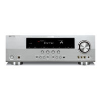
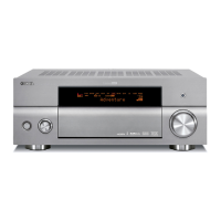
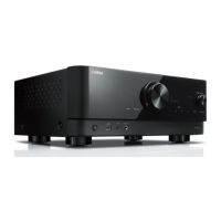
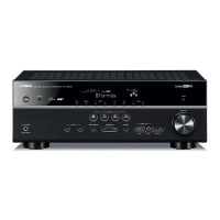
Illustration of the front panel layout for RX-V463 (U, C models).
Illustration of the front panel layout for RX-V463 (R, T, K, A, G, E, F models).
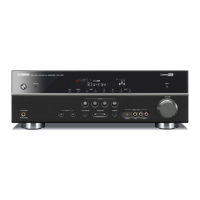
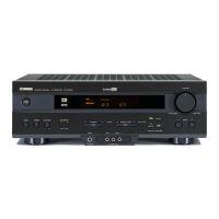
Illustration of the front panel layout for HTR-6140 (U, C models).
Illustration of the front panel layout for HTR-6140 (T, K, G, E, F models).
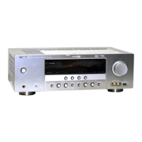
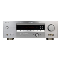
Illustration of the front panel layout for DSP-AX463 (B model).
Illustration of the front panel layout for DSP-AX463 (J model).
Illustration of the rear panel layout for RX-V463 (U, C models).
Illustration of the rear panel layout for RX-V463 (R model).
Illustration of the rear panel layout for RX-V463 (T model).
Illustration of the rear panel layout for RX-V463 (K model).
Illustration of the rear panel layout for RX-V463 (A model).
Illustration of the rear panel layout for RX-V463 (G, E, F models).
Illustration of the rear panel layout for RX-V463 (L model).
Illustration of the rear panel layout for HTR-6140 (U, C models).
Illustration of the rear panel layout for HTR-6140 (T model).
Illustration of the rear panel layout for HTR-6140 (K model).
Illustration of the rear panel layout for HTR-6140 (G, E, F models).
Illustration of the rear panel layout for DSP-AX463 (B model).
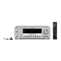
Details and image of the RAV280 remote control.
Details and image of the RAV281 remote control.
Details and image of the RAV282 remote control.
Comprehensive specifications for the audio performance and parameters of the unit.
Comprehensive specifications for the video signal processing and parameters.
Specifications related to the FM tuner reception sensitivity and signal quality.
Specifications related to the AM tuner reception range and input.
General specifications including power supply voltage and consumption details.
Physical dimensions of the unit in millimeters and inches.
The weight of the unit in kilograms and pounds.
List of available color finishes for different model variations.
List of accessories provided with the unit.
Template for setting up various scene modes for different input sources.
Menu options for selecting sound fields and surround decoder parameters.
Settings related to audio adjustments, speaker configuration, and sound modes.
Options for assigning and renaming input sources and managing decoder modes.
Configuration settings for display, memory, audio selection, and system initialization.
Diagram showing the internal layout of components from the top perspective.
Diagram illustrating internal components viewed from the front.
Diagram showing internal components as seen from the rear.
Step-by-step instructions for removing the top cover of the unit.
Instructions for detaching and removing the front panel unit.
Procedure for removing the DSP P.C.B., including notes on model ID settings.
Instructions for removing the VIDEO (1) and (2) printed circuit boards.
Procedure for removing the VIDEO (4) printed circuit board.
Steps for removing the FM/AM tuner module from the unit.
Crucial instruction to connect ground leads to the chassis for proper PCB function after removal.
Requirement to write the latest firmware after replacing specific circuit boards or ROMs.
List of tools and media required for the firmware update process.
Step-by-step instructions for performing the firmware update using a DVD/CD player.
Procedure to activate the FIRMWARE UPDATE mode by pressing specific keys.
Instructions for connecting the power for the external DVD/CD player.
Indicates the start of the firmware writing process, showing the address.
Shows the completion status of the firmware writing process with success messages.
Describes the scenario where firmware versions match, negating the need for an upgrade.
Troubleshooting steps if the display does not change during firmware CD playback.
Troubleshooting steps if a "FILE CORRUPTED" message appears during the update.
Procedure to initialize the unit after a firmware update is completed.
Method to confirm successful firmware update by checking version and checksum via self-diagnostic menu.
Steps to navigate the self-diagnostic menu to check the firmware version.
Steps to navigate the self-diagnostic menu to check the overall checksum.
Steps to navigate the self-diagnostic menu to check the program checksum.
Final step to power off the unit after confirmation.
Procedure to set the M6 Model ID for EDID settings after firmware changes.
Method to select the correct model name using preset tuning keys.
Explains the unit's self-diagnostic capabilities for inspection and fault finding.
Important note stating that not all diagnostic menu items may be applicable to all models.
Lists the main menu categories within the self-diagnostic function.
Instructions on how to start the self-diagnostic function by pressing specific keys.
Procedure to start diagnostics with protection functions disabled for troubleshooting.
Steps to cancel the self-diagnostic function and return to normal operation.
Describes the initial display messages when the self-diagnostic function starts.
Indicates the display message when no protection history is recorded.
Explains the cause of protection activation due to excessive current in the power amplifier.
Critical notes on the dangers of operating with protection disabled and checking output transistors.
Details protection activation caused by abnormal voltage in the power supply section.
Explains protection activation due to abnormal DC output from the power amplifier.
Describes protection activation caused by excessive heat sink temperature.
Information on how protection history is stored in memory and how it can be cleared.
How the FL display indicates the function currently being operated.
Instructions on how to navigate the main and sub-menus within the diagnostic function.
Lists additional functions available during self-diagnostic mode, like volume and muting control.
Details the default settings applied when starting the self-diagnostic function.
Details the BYPASS function, allowing selection of Analog or DSP bypass output.
Describes how analog input signals are output without effects.
Describes how digital input signals are output without effects.
Explains the AUDIO CHECK function, outputting input sound signals.
Explains the analog switch settings for speaker configuration options.
Details the 'LARGE' speaker setting for high bass performance speakers.
Details the 'SMALL' speaker setting for low bass performance speakers.
Explains the 'NONE' setting for when no center speaker is used.
Details the XCH INPUT selection for multi-channel sources.
Specific sub-menu option for 6-channel input with 6-ohm impedance.
Specific sub-menu option for 8-channel input with 6-ohm impedance.
Specific sub-menu option for 6-channel input with 8-ohm impedance.
Explains the MIC CHECK function for testing microphone input signals.
Details parameters for Limiter Control, Power Limiter Detection, and Thermo Protection.
Describes the FL/OSD CHECK program for testing the front display section.
Explains the TEST TONE function for outputting noise through specified channels.
Describes the XM STATUS check for XM radio execution.
Note indicating that XM STATUS is not applicable to this model.
Explains the iPod menu for testing the DOCK connector without the iPod connected.
Information on the DOCK connector test items and results.
Describes the DOCK ignore function, disabling the DOCK input source.
Displays the firmware version of the Bluetooth module when connected.
Options to inhibit or reserve the clearing of Bluetooth DOCK pairing information.
Explains the USB function for reproducing music files from a flash memory.
Indicates playback of the first music file from the connected USB flash memory.
Indicates playback of the second music file from the connected USB flash memory.
Describes the SIRIUS antenna module check.
Checks the connection status of the SIRIUS antenna module.
Displays connection information for the SIRIUS antenna module.
Performs a SIRIUS loop-back test for diagnostic purposes.
States that VIDEO CONVERSION is not applicable to these models.
Displays video information, but the function is not applicable.
Allows selection of input signals to be output via HDMI OUT.
Outputs SPDIF signal for audio playback via HDMI.
Indicates that no signal is output via HDMI.
Indicates that HDMI "IN 1" is output.
Indicates that HDMI "IN 2" is output.
Performs an I2C access check to verify data read/write operations.
Procedure to set the M6 Model ID for EDID settings after firmware changes.
Displays A/D conversion values for panel keys and protection functions.
Parameters for Power Amplifier DC Protection (PD) and DOCK ID detection (DI).
Parameters for Voltage Protection (V1, V2) detection.
Parameters for Thermo Protection (TH) and Power Limiter detection (PL).
Parameters for Current Protection (PI) and Sub-trans voltage detection (DE).
Checks the A/D values of panel keys to ensure proper function.
Displays the A/D setting values for each protection function.
Displays the history of protection events that have occurred.
Indicates a reserved menu item, not detailed here.
Options to reserve or inhibit user memory initialization to factory settings.
Cautionary note about backing up tuner memory before setting PRESET RESERVED.
Displays the firmware version and checksum, processed with EFFECT OFF.
Displays the firmware version of the microprocessor.
Displays the checksum value of the microprocessor.
Displays the checksum value for the application and standby code.
Displays the checksum value for the SPI firmware update code.
Displays the checksum value for the SPD firmware update code.
Table showing anode connections for various pins.
Table detailing pin numbers and their connections.
Diagram showing grid assignments for display segments.
Block diagram and pin assignments for the digital audio interface transceiver IC.
Notes on withstand voltage input/output levels for pins.
Information on using pins 32 and 33 for chip address setting.
Describes pin 34's role in demodulation or master/slave settings.
Pin 35's function for modulation or general I/O settings.
Critical instruction on timing power supply ON/OFF to prevent latch-up.
Describes the JTAG test and emulation interface.
Details the event controller and core timer functionalities.
Information about the real-time clock feature.
Description of the UART port with IrDA support.
Details the serial port (2) functionality.
Information about the SPI port interface.
Describes control of external FLASH and SDRAM.
Details the memory interface for asynchronous and synchronous access.
Control functions for asynchronous memory access.
Control functions for synchronous memory access.
Information on the timer functions.
Details about the PPI port and its functions.
Description of Port F, covering GPIO, PPI, SPI, and timers.
Details the pins and functions of the JTAG port.
Details the pins and functions of the SPI port.
Details the pins and functions for serial ports (SPORT0, SPORT1).
Details the pins and functions of the UART port.
Details the pins and functions for the real-time clock.
Details the pins and functions for clock input/output.
Details the pins for mode control, including reset and boot mode.
Details the pins related to the voltage regulator.
Details the pins providing I/O power supply.
Details the pins providing core power supply.
Details the pins providing power for the real-time clock.
Details the pins for external ground connection.
Pin assignments and functions for IC57, an octal flip-flop.
Pin assignments and functions for IC58, an octal flip-flop.
Pin assignments and functions for IC56, an octal flip-flop.
Pin assignments and functions for IC59, an octal flip-flop.
Pin connections and function names for the ADC IC81.
Details key detection for the A/D port, including pull-up resistance.
Pin assignments and functions for IC82 and IC83, analog multiplexers.
Details DOCK detection for AD port, including pull-up resistance.
Describes the MCU interface for IC401.
Explains the function of connecting capacitors for click noise reduction.
Identifies output pins for volume signals across multiple channels.
Describes the analog ground connections within the circuit.
Pin for setting frequency characteristics of tone control (Bass).
Pin for setting frequency characteristics of tone control (Treble).
Pin for controlling the outside mute function.
Pin used as an input selector for L/R channels.
Block diagram of the display controller for the VFD.
Circuit for receiving serial data.
Circuit for outputting digit data to the VFD.
Block for generating clock signals.
Details pins designated for segment output.
Details pins designated for digit output.
Instruction to connect specific pins to VFD segment (anode) pins.
Instruction to connect specific pins to VFD digit (grid) pins.
Block diagram illustrating the audio signal path and digital processing sections.
Reference to schematic diagrams for DSP related sections.
Block diagram detailing the DSP control section and its interconnections.
Block diagram showing analog audio paths and the power supply system.
Block diagram illustrating the video signal processing and input/output paths.
Block diagram showing the overall control signals and system interconnections.
Layout diagram of the DSP P.C.B. (Side A) with semiconductor locations.
Table detailing the location of semiconductors on the PCB.
Layout diagram of the DSP P.C.B. (Side B).
Layout of the OPERATION (1) P.C.B. (Side A) with component references.
Table detailing semiconductor locations on the OPERATION (1) P.C.B.
Layout of the OPERATION (1) P.C.B. (Side B).
Layout of the OPERATION (2) P.C.B. (Side A) with semiconductor locations.
Table detailing semiconductor locations on the OPERATION (2) P.C.B.
Layout of the OPERATION (2) P.C.B. (Side B).
Layout of the OPERATION (3) P.C.B. (Side A).
Layout of the OPERATION (3) P.C.B. (Side B).
Layout of the OPERATION (4) P.C.B. (Side A).
Layout of the OPERATION (4) P.C.B. (Side B).
Layout of the OPERATION (5) P.C.B. (Side A).
Layout of the OPERATION (5) P.C.B. (Side B).
Layout of the OPERATION (6) P.C.B. (Side A).
Layout of the OPERATION (6) P.C.B. (Side B).
Layout of the OPERATION (7) P.C.B. (Side A).
Layout of the OPERATION (7) P.C.B. (Side B).
Layout of the OPERATION (8) P.C.B. (Side A).
Layout of the OPERATION (8) P.C.B. (Side B).
Layout of the OPERATION (9) P.C.B. (Side A).
Layout of the OPERATION (9) P.C.B. (Side B).
Layout of the MAIN (1) P.C.B. (Side A) with component locations.
Layout of the MAIN (2) P.C.B. (Side A).
Layout of the MAIN (1) P.C.B. (Side B).
Layout of the MAIN (2) P.C.B. (Side B).
Layout of the VIDEO (1) P.C.B. (Side A) with semiconductor locations.
Table detailing semiconductor locations on the VIDEO (1) P.C.B.
Layout of the VIDEO (1) P.C.B. (Side B).
Layout of the VIDEO (2) P.C.B. (Side A) with semiconductor locations.
Table detailing semiconductor locations on the VIDEO (2) P.C.B.
Layout of the VIDEO (2) P.C.B. (Side B).
Layout of the VIDEO (3) P.C.B. (Side A) with semiconductor locations.
Table detailing semiconductor locations on the VIDEO (3) P.C.B.
Layout of the VIDEO (3) P.C.B. (Side B).
Layout of the VIDEO (4) P.C.B. (Side A).
Table detailing semiconductor locations on the VIDEO (4) P.C.B.
Layout of the VIDEO (5) P.C.B. (Side A) with voltage selector details.
Pin connection diagrams for various integrated circuits (ICs).
Pin connection diagrams for diodes.
Pin connection diagrams for various transistors.
Schematic diagram section for the DSP, part 1 of 8.
Schematic for IC11, an HDMI/DVI transmitter.
Schematic for IC12, a video decoder.
Schematic for IC13, a low dropout voltage regulator.
Schematic for IC31, a digital audio interface transceiver.
Schematic for IC38, an audio digital-to-analog converter.
Schematic for IC39, a stereo A/D converter.
Schematics for IC33 and IC34, quadruple data selectors.
Schematic diagram section for the DSP, part 2 of 8.
Schematic for IC22, a low dropout voltage regulator.
Schematic diagram section for the DSP, part 3 of 8.
Schematic for IC31, a digital audio interface transceiver.
Schematic for IC38, an audio digital-to-analog converter.
Schematic for IC39, a stereo A/D converter.
Schematics for IC33 and IC34, quadruple data selectors.
Schematic diagram section for the DSP, part 4 of 8.
Schematic for IC41, the main microprocessor.
Schematic for IC42, the EEPROM.
Schematics for IC43 and IC44, dual 4-channel multiplexers.
Schematic diagram section for the DSP, part 5 of 8.
Schematic for IC51, a synchronous DRAM.
Schematic for IC155, hex schmitt trigger inverters.
Schematic for IC152, quadruple 2-input OR gates.
Schematic for IC153, quadruple 2-input AND gates.
Schematic for IC154, dual monostable multivibrators.
Schematic for IC52, a 16 M-bit flash memory.
Schematics for IC53-55 and IC151, octal bus transceivers.
Schematic for IC56, octal flip-flops.
Schematic diagram section for the DSP, part 6 of 8.
Schematic for IC62, octal bus transceivers.
Schematic diagram section for the DSP, part 7 of 8.
Schematic for IC71, a USB host controller.
Schematic for IC72, octal bus transceivers.
Schematic for IC73, a high-side switch IC.
Schematic diagram section for the DSP, part 8 of 8.
Schematic for IC81, an A/D converter.
Schematics for IC82 and IC83, analog multiplexers.
Schematic diagram section for the operation circuits, part 1 of 2.
Schematic for IC601, a dual operational amplifier.
Schematic for IC603, a VFD controller/driver.
Schematic diagram section for the operation circuits, part 2 of 2.
Schematics for IC701 and IC703, voltage regulators.
Schematic for IC704, a voltage regulator.
Schematic for IC705, a voltage regulator.
Schematic for IC708, a temperature sensor.
Schematic for IC706, a low dropout voltage regulator.
Schematic for IC707, a low dropout voltage regulator.
Schematic diagram section for the main board, part 1 of 2.
Schematic for IC501, a 3-channel AF power amplifier.
Schematic for IC502, a 2-channel AF power amplifier.
Schematic diagram section for the main board, part 2 of 2.
Schematics for IC403-405 and IC407, dual operational amplifiers.
Schematic for IC402, an RDS signal demodulation IC.
Schematic diagram section for video circuits, part 1 of 2.
Schematic for IC308, a voltage regulator.
Schematic for IC309, a voltage regulator.
Schematic for IC307, a 6-channel video driver.
Schematic for IC304, an OSD controller.
Schematic for IC301, an 8-channel analog multiplexer.
Schematic for IC311, an analog multiplexer/demultiplexer.
Schematic diagram section for video circuits, part 2 of 2.
Schematic for IC325, a video amplifier.
Schematics for IC322-324, analog multiplexers.
List of electrical components with part numbers and descriptions.
Warning regarding special characteristic parts and the unavailability of chip resistors as replacements.
Parts list for the DSP P.C.B., including reference numbers and descriptions.
Continuation of the parts list for the DSP P.C.B.
Further continuation of the parts list for the DSP P.C.B.
Additional entries in the parts list for the DSP P.C.B.
Parts list for the MAIN and VIDEO P.C.B.s.
Parts list for the OPERATION P.C.B.s.
Continuation of the parts list for the OPERATION P.C.B.
Parts list for the MAIN P.C.B.
Continuation of the parts list for the MAIN P.C.B.
Further continuation of the parts list for the MAIN P.C.B.
Parts list for the MAIN and VIDEO P.C.B.s.
Parts list for the VIDEO P.C.B.
Continuation of the parts list for the VIDEO P.C.B.
Note indicating that certain chip resistor values are not available.
Exploded view of the front panel unit assembly.
Exploded view of the amplifier unit assembly.
List of included accessories such as remote control, antennas, and batteries.
Part numbers for various P.C.B. assemblies (DSP, MAIN, VIDEO).
Part number and description for various front panel parts.
Part number and description for a button case.
Part number and description for a button tuner.
Part number and description for an emblem.
Part number and description for an escutcheon.
Part number and description for a window sheet.
Part number for OPERATION P.C.B. assembly.
Part number for a flexible flat cable.
Part number for MAIN P.C.B. assembly.
Part number for OPERATION P.C.B. assembly.
Part number for a flexible flat cable.
Part number for screws.
Lists the remote control models covered.
Schematic diagram of the remote control circuit.
Panel layouts for the different remote control models.
Diagram showing the key layout on the remote control.
Table listing IR codes for various keys and functions across different remote models.
Function chart detailing the actions of various remote control buttons.
Instructions on how to configure advanced settings.