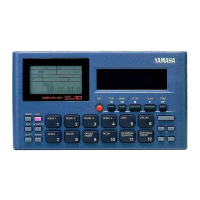
SPX50D
SPX50D
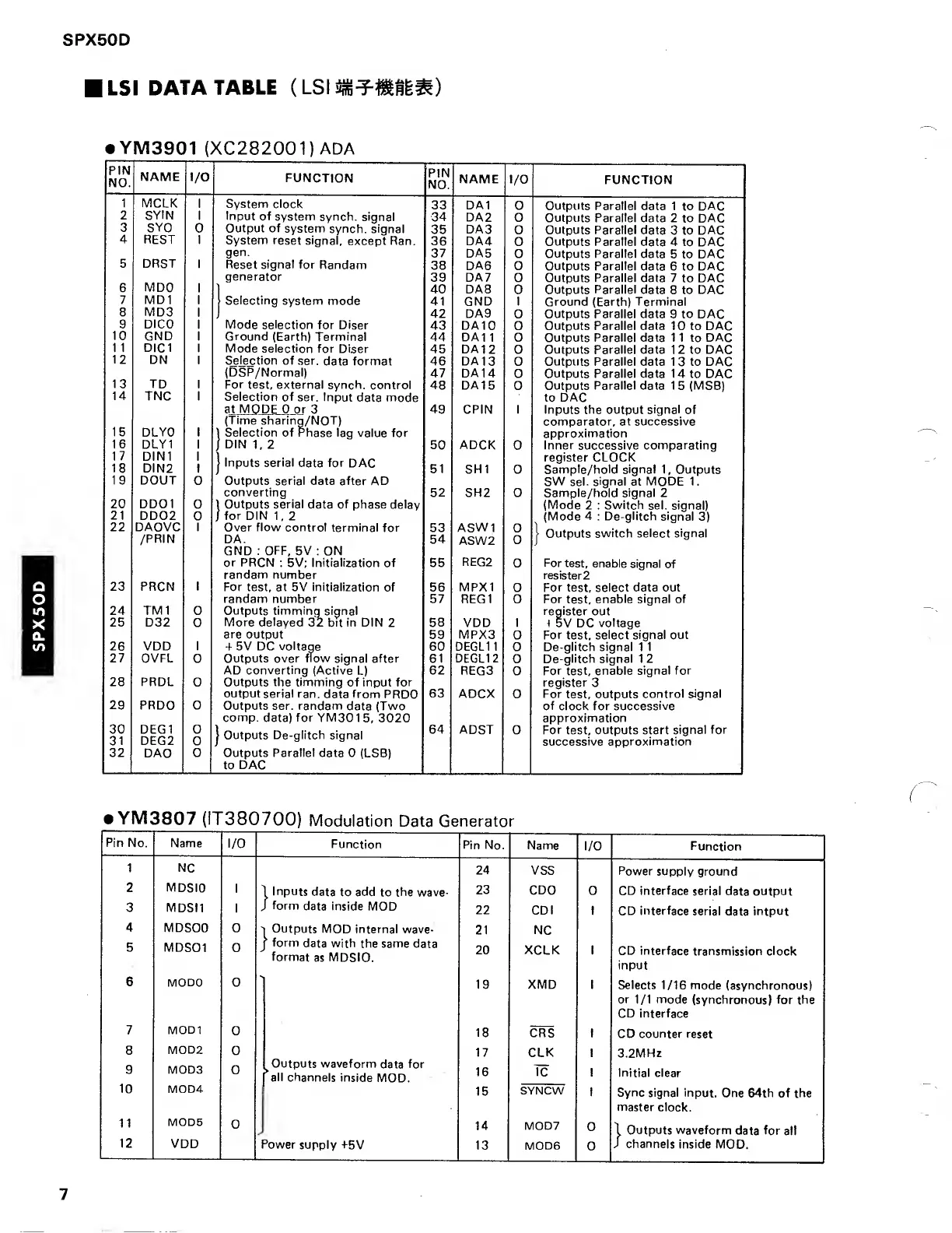
LSI
DATA
TABLE
• YM3901
(XC28200DADA
FUNCTION
PIN
NO.
NAME I/O
FUNCTION
1
MCLK
1 System
clock
33
DAI
0 Outputs Parallel
data 1 to DAC
2 SYIN
1 Input
of
system synch,
signal 34
DA2
0 Outputs Parallel
data 2 to DAC
3 SYO
0
Output of
system synch, signal
35
DA3
0
Outputs
Parallel data
3 to
DAC
4
REST
1
System reset
signal,
except Ran.
36 DA4
0
Outputs
Parallel data 4 to DAC
DRST
gen.
37 DA5
0
Outputs
Parallel data
5 to
DAC
5
1
Reset signal for
Randam
38 DA6
0 Outputs Parallel
data 6 to DAC
MDO
generator
39
DA7
0 Outputs Parallel data 7
to
DAC
6
1
40 DA8
0
Outputs
Parallel
data
8 to
DAC
7 MD1
1
}
Selecting
system
mode
41 GND 1
Ground (Earth)
Terminal
8 MD3
1
)
42 DA9
0
Outputs Parallel
data 9
to
DAC
9 DICO
1 Mode selection
for Diser
43
DA10
0
Outputs
Parallel
data
10 to DAC
10 GND
1 Ground (Earth)
Terminal
44 DAI
1 0 Outputs Parallel data 1 1 to DAC
1 1 DIC1 1 Mode
selection for
Diser
45 DAI
2 0
Outputs
Parallel data 12 to DAC
12
DN
1 Selection
of ser.
data format
46
DA13
0
Outputs
Parallel data 13 to DAC
13
(DSP/Normal)
47
DA14
0 Outputs Parallel data 14 to
DAC
TD
1 For test,
external synch,
control 48 DA15
0
Outputs Parallel data
15
(MSB)
14
TNC 1
Selection
of ser. Input
data mode to DAC
at
MODE
0 or 3 49
CPIN 1 Inputs the output signal
of
(Time
sharing/NOT)
comparator, at successive
15 DLYO
1
\
Selection
of Phase lag
value for
approximation
16
DLY1 1
/
DIN
1,
2
50 ADCK
0
Inner successive comparating
17
18
DIN1
DIN2
1
1
1
Inputs serial
data for
DAC
51 SHI
0
register
CLOCK
Sample/hold signal
1,
Outputs
19 DOUT
0 Outputs serial data after AD
SW sel.
signal
at
MODE 1
.
20 DD01
converting
52
SH2 0 Sample/hold signal 2
0
\
Outputs serial
data
of
phase
delay
(Mode
2 :
Switch
sel. signal)
21
DD02
0
/for DIN
1,
2 Mode
4
: De-glitch signal
3)
22 DAOVC
/PRIN
1 Over flow control
terminal for
DA.
53
54
ASW1
ASW2
0
0
1
\
Outputs switch select
signal
GND : OFF, 5V
: ON
or PRCN
: 5V;
Initialization
of 55
REG2
0
Eor
test,
enable
signal
of
randam number
resister
2
23 PRCN 1
For test, at 5V initialization
of 56
MPX1
0
For test, select data out
randam number 57
REG1 0 For test,
enable signal of
24
TM1
0
Outputs
timming signal
More delayed
32 bit in DIN
2
register
out
25 D32
0
58
VDD 1 t
5V DC
voltage
are
output
59 MPX3
0
For
test,
select signal out
26 VDD 1
4
5V DC voltage
60 DEGL11
0 De-glitch signal 1 1
27 OVFL
0
Outputs over
flow
signal after
61
DEGL12
0
De-glitch signal 1 2
AD
converting
(Active
L)
62
REG3
0
For test, enable
signal for
28 PRDL
0
Outputs the timming
of input
for
register
3
output
serial ran.
data
from
PRDO
63
ADCX
0
For
test, outputs
control signal
29
PRDO 0 Outputs
ser. randam
data (Two
of
clock for
successive
30
31
DEG1
DEG2
comp,
data)
for YM301
5,
3020
approximation
0
0
1
Outputs De-glitch signal
64
ADST
0
For
test,
outputs
start
signal for
successive approximation
32
DAO
0 Outputs Parallel data
0
(LSB)
to
DAC
• YM3807
(1T380700)
Modulation
Data Generator
Pin
No.
Function
^Outputs waveform
data for
all
channels inside
MOD.
Power
supply
+5V
Pin
No.
\
Inputs
data
to
add
to the wave-
/
form
data inside
MOD
t Outputs MOD
internal wave-
J
form
data
with the same data
format
as MDSIO.
Function
Power supply
ground
0 CD interface
serial
data
output
1 CD interface
serial
data
intput
CD interface
transmission
clock
input
Selects
1/16 mode (asynchronous)
or
1/1
mode
(synchronous)
for
the
CD
interface
CD counter reset
3.2MHz
Initial clear
Sync
signal input.
One 64th
of the
master
clock.
channels
inside MOD.
 Loading...