3 Terminals
3.1 Main circuit terminals
・As the VS mini J7 and J1000 may have different terminals sizes (depending on capacity), this point
has to be carefully checked before the replacement (see 3.4).
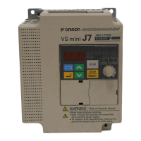
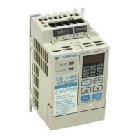
J7
Main terminals
J1000
Main terminals
Note
R/L1 R/L1
S/L2 S/L2
T/L3 T/L3
Power supply connection.
Note:
In the J7 the power supply terminals are located at the top
of the drive. In the J1000 they are located at the bottom.
Make sure the cables fit without tension. Replace or extend
them if needed.
U/T1 U/T1
V/T2 V/T2
W/T3 W/T3
Drive output
- B1 Braking resistor or external braking chopper connection
- B2 Braking resistor connection
+1 +1 DC Reactor connection, DC power supply input
+2 +2 DC Reactor connection
− −
DC power supply input, external braking chopper connection
Ground connector (ground with <100Ohm for 200 V class
and < 10 Ohm for 400 V class)
3.2 Control Terminals, Signal Levels
Te rm ina l
Signal Level
J7 J1000
Function
J7 J1000
S1
Multi function input 1
(1: Run forward 0: Stop)
S2
Multi function input 2
(1: Run reverse 0: Stop)
S3
Multi function input 3
(J7: Fault Reset / J1000: Ext. Fault)
S4
Multi function input 4
(J7: Ext. Fault / J1000: Fault Reset)
S5
Multi function input 5 (Multi speed 1)
Photo coupler isolation
24 Vdc,8 mA
Photo coupler
24 Vdc,8 mA
SC
Multi function input common
- -
FS +V
Analog input power supply
+12 Vdc, max. 20 mA +10.5 Vdc, max. 20 mA
FR A1
Analog input 1
(frequency reference)
0-10 Vdc (20 kΩ),
0 or 4-20 mA (250 Ω),
0-10 Vdc (20 kΩ),
0 or 4-20 mA (250 Ω)
FC AC
Analog input common
0V
MA
Change over contact output (NO)
(Fault)
MB
Change over contact output (NC)
(Fault)
MC
Change over contact output common
Max. load
250 Vac 1 A max.
30 Vdc 1 A max.
Max. load
250 Vac 10 mA〜1A
30 Vdc 10 mA〜1A
AM
Analog output
AC
Analog output GND
0-10 Vdc,max. 2 mA
Resolution 8 Bit
0-10 Vdc,max. 2 mA
Resolution 8 Bit
3.3 DIP Switches
When replacing a J7, make sure to set the DIP switches S1 and S3 on the J1000 properly.
VAN-V07007E [J7→J1000] Replacement Instructions
4/16
J7 J1000
Function
Switch Default Switch Default
NPN/PNP selection
SW7 NPN S3 NPN
Analog input 1 level sel.
SW8 Voltage S1 Voltage
 Loading...