SR23 - 923-03509 3-9 CS - SERVICING
CIRCUIT OVERVIEW (continued)
When QX3200 is turned off, about 1100 Volts peak of
flyback voltage is produced from the stored energy in
the horizontal deflection coils and T3201. This voltage
is induced to secondary windings of T3201 to generate
the high voltage from 28 to 30 KV. The flyback (or
retrace) period is about 5 µs.
A secondary winding on T3201 (pin 6) provides a low
voltage flyback pulse (H-FLYBK) used for synchronization
of the Scan Boost Converter and like a feedback signal
for the HV Compensation circuit. A capacitive divider,
CX3216 and CX3217, provides a low voltage flyback pulse
(H-FBP) used for synchronization, phase comparison,
etc. This pulse is sent to the main chassis via pin 6 of
connector 4G2.
Linearity Coil, L3200, is a saturating inductor skewed
by a permanent magnet bonded to the coil. It produces
a nonlinear inductance curve versus the current. This
characteristic cancels non-linear ties in the deflection
current caused by horizontal deflection coil resistance.
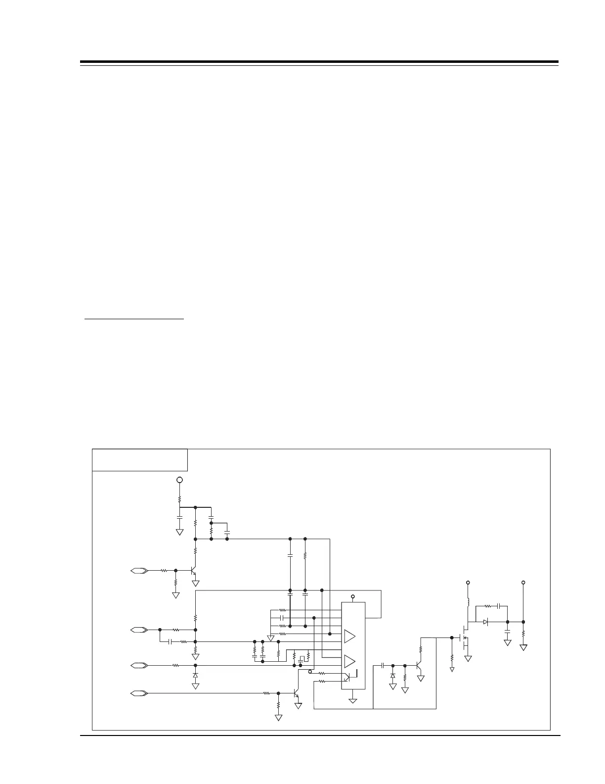
SCAN BOOST CONVERTER
Because the horizontal scan frequency is not constant,
a variable voltage source is required to supply the main
deflection circuit. The Scan Boost Converter circuit
accomplishes this. The +40 Vdc Power Supply (from main
switched mode power supply in the chassis) is boosted
to the voltage required for a given operating frequency
and becomes the B++ voltage to supply the main
deflection circuit. The scan converter is a pseudo-
synchronized, PWM, discontinuous, flyback type.
Pulse width modulation control is achieved by IC4100.
It’s function is to modulate the pulse width output at
pin 8 based on the error voltage resulting from
comparing the reference voltage at pin 2 with that at
pin 1.
Scan converter free run operating frequency is controlled
by R4120 and C4103. It is necessary to synchronize
this frequency with the incoming Horizontal Scanning
Frequency. Q4101 provides injection locking of the
oscillator by discharging C4103 during the horizontal
retrace interval, after which the oscillator is allowed to
free run only during the remaining scanning period.
The effect is a pseudo-sync-locked oscillator. This
provides improved noise and response performance,
while reliably operating in the discontinuous mode over
the entire horizontal operating frequency range.
The output at pin 8 drives the gate of the switching
transistor Q4103. The on interval determines the amount
of stored energy in L4100. The longer Q4103 is on, the
more energy is stored, resulting in a higher rectified
output voltage at B++ after Q4103 is turned off. Q4102
provides a fast turn off of Q4103.
Scan Boost Converter
B++
R4103
C4104
R4104
C4105
C4117
R4105
R4102
R4100
R4101
Q4100
R4107
R4408
C4100
R4106
R4109
R4120
C4103
R4114
R4113
R4110
R4111
C4101
C4102
R4112
R4130
D4100
R4116
C4106
R4115
C4107
R4117
+15V
10
VCC
6
5
4
1
2
3
14
13
9
8
R4122
R4123
+15V
Q4101
R4118
R4119
GND
+
1
-
+
2
-
R1
C1
OTC
PWMCOMP
C4111
D4101
R4125
Q4102
R4126
Q4103
L4100
RX4127
C4113
C4115
D4102
RX4128
B+
+40V
IN
IN
IN
IN
H-FLBK
FH-STAT
EW-DRV
F0
IN
0
0
7
0
0