SR23 - 923-03509 3-8 CS - SERVICING
CIRCUIT OVERVIEW (continued)
DEFLECTION AND HIGH VOLTAGE
OVERVIEW
The principal function of the Deflection and HV circuits
is to supply horizontal and vertical currents to the
deflection yoke coils, and the high voltage generation.
They are designed for use in a dual frequency television,
15.75 and 37.9 Khz. They are dependent on other
circuits in the chassis to provide drive signal, DC control
voltages, correction waveform, etc. This section can be
divided into 7 functional blocks.
1. Horizontal Deflection and HV Generation
2. Scan Boost Converter
3. Base Drive
4. S-Capacitor Switched
5. HV Compensation
6. Shutdown Circuit
7. Vertical Deflection
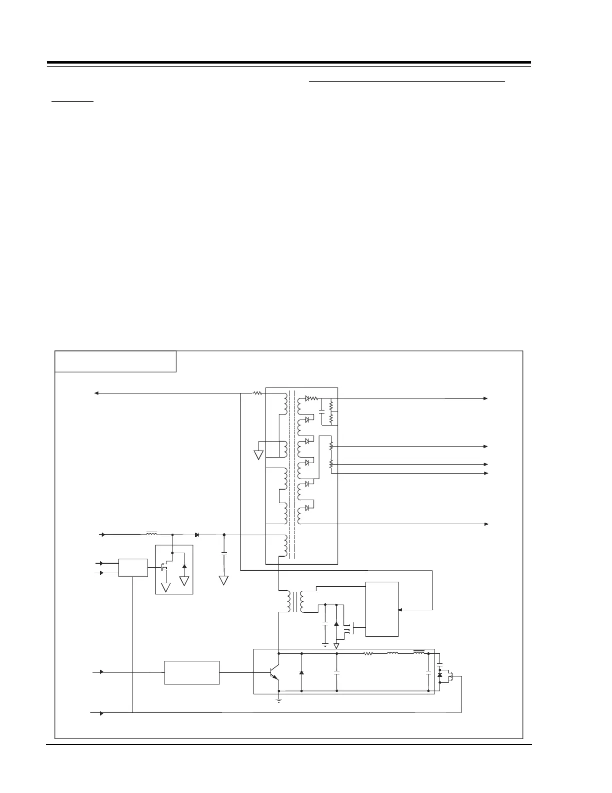
HORIZONTAL DEFLECTION AND HV GENERATION
The Horizontal Deflection circuitry is a common flyback
type used in many television and monitor applications.
QX3200 is the Horizontal Output Transistor. When QX3200
is initially turned on, current is allowed to flow from
the B+ supply, through TX2900, T3201, and QX3200.
This allows energy to be stored in T3201. When QX3200
is turned off, some of this energy is returned to charge
the S-capacitor(s) CX3203, CX3204, and CX3205. After
several cycles (repeating at scanning frequency)
sufficient voltage appears across the S-capacitor
providing an additional path producing current flow
though the horizontal deflection yoke coil (connector
4X4). The Damper Diode DX3200 provides the negative
current path. The result is a positive and negative
sawtooth current through the horizontal deflection coils
(approximately 11 to 17 Amps. peak to peak).
D3200X
Q3200X
Proportional
H-Drive
Yoke
T3202
T3201
Sweep
Transformer
PWM
Scan Boost
Converter
HV
F1
G2
GF
ABL
H-DRIVE
F0
40 VDC
HFLBK SHUTDOWN
High Voltage & Deflection
E/W-DRV
FH-STAT