SR23 - 923-03509 3-11 CS - SERVICING
CIRCUIT OVERVIEW (continued)
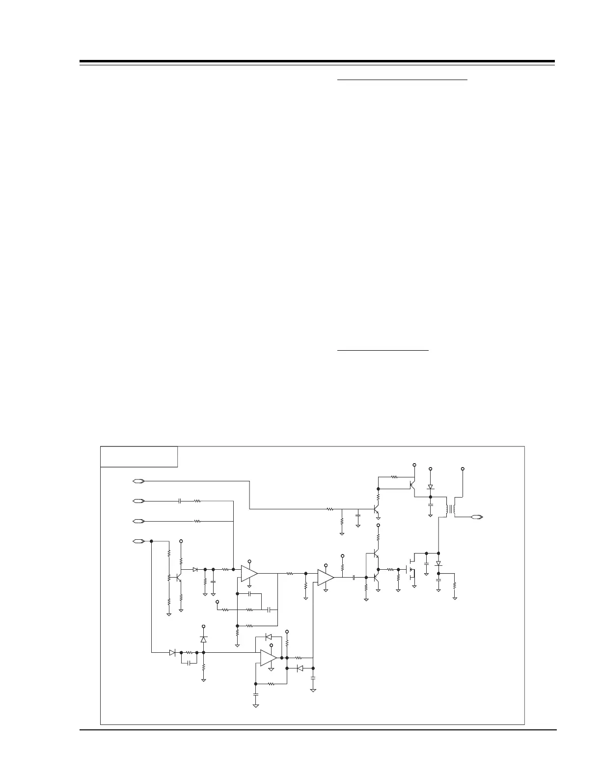
The error voltage is compared with a ramp signal
generated in one comparator of IC2900 and
synchronized by the flyback pulse (H-FLYBK) at
Horizontal Scanning Frequency. It modulates the pulse
width in the output to drive the gate of the switching
transistor Q2904. This ramp signal is present only
during the flyback pulse.
Q2904 is on during the scan time and as long as the
error voltage is higher than the ramp signal. This allows
energy to be stored in TX2900. When Q2904 is turned
off the resonant circuit formed by C2908 and the primary
inductance of TX2900 produce a flyback voltage of about
400 volts peak resulting from the store energy in TX2900.
This voltage is induced to secondary windings of TX2900
to add to voltage generated in Horizontal Deflection
circuit. This induce voltage is used to compensate load
variation (beam current variation) in HV Flyback
Transformer T3201. ABL and EW-DRV signals, weighted,
can be used to ameliorate the HV controller response.
Q2905 and Q2906 are used, with F0 signal from the
Deflection Processor (ICX2600 in Main Chassis), to
switch +22V or +40 V to pin 4 of TX2900 to maintain
the same energy stored in TX2900 for both modes (NTSC
and SVGA).
Q2900 and RX2952 (potentiometer) are used to adjust
the high voltage to a specified level and for coupling
with HV controller (IC3201.
SHUTDOWN CIRCUIT OPERATION
The flyback pulse voltage from pin 6 of T3201 (Flyback
Transformer) is peak detected (rectified) by the action
of diode D3206 and capacitor C3214. This forms a DC
voltage appearing on C3214 representative of the CRT
anode voltage (HV) procedure by T3201. This voltage
is divided down precision resistors RX3214, RX3215,
RX3216, and RX3217. This lower voltage appears on
the positive input (pin3) of IC3201. In the event the
CRT anode voltage become excessive, in IC3201 the
positive input (pin3) will be higher that negative input
(pin2) and therefore his output (pin1) will go to high
level at approximately 15 volts. This signal (SD-DVR) is
send to Base of Q4000 causing Horizontal Drive to be
disabled and latched causing HV goes down. In about
5 seconds, the shutdown-reset circuit (Pins 8,9 & 14
of IC2900) enabled again the Horizontal Drive and HV
must be reestablished.
The circuit formed by Q2907, C2913, C2916, D2908,
R2923, R2935, R2936 and R2937; disable the HV
compensation output (Q2902-B signal) during turn on
and shutdown conditions (transients).
VERTICAL DEFLECTION
The Vertical Deflection circuit, ICX2100, is a linear
amplifier that can directly drive the yoke current
(including the required DC component). The sawtooth
waveforms needed, as inputs, by ICX2100 are generated
in the Deflection Processor, ICX2600, in Main Chassis,
V-DRV+ and V-DRV, pin 1 and 2 of connector 4V2.
IN
IN
IN
IN
F0
EW-DRV
ABL
H-FLYBK
C2902
R2907
R2931
R2903
RX2900
RX2901
RX2902
RX2904
Q2900
D2901
R2905 C2900
R2906
+15V
+15V
V+
V-
IC3201
C2915
R2911R2914
+5V
C2903
R2915
R2917
R2912
R2913
+15V
C2906
R2919
R2918
R2922
C2912
+15V
D2902
D2903
V+
V-
IC2900
+
-
+
-
+
-
V+
V-
IC2900
R2920
R2921
+15V
D2905
D2902
C2907
3
2
3
2
3
2
+15V
C2913
8
4
8
4
8
4
+15V
R2923
R2925
R2931
R2931
C2915
Q2905
R2933
R2934
+15V
+40V
RX2926
Q2904
Q2903
RX2929
R2928
D2904
C2908
Q2906
C2914
R2930
OUT
L2L1
C2911
Q2906
D2907
+22V
B++
0
0
0
0
0
0
0
0
0
0 0
0
0
0
0
0
0
0
0
0
HV Compensation