25
6-3. Fuses Replacement
If occasion should require replacement of the mains fuses, use only standard ones.
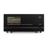
The two Primary Mains Fuses of the amplifier are located on the rear panel (Fig. 2.2).
They are 20A/250V Quick blow, 1-1/4 x 1/4 inch Cartridge Fuses, Size "0" Ceramic.
Besides the primary fuses, on the MAINS CONTROL BOARD there are six small glass fuses (5x20mm)
which are not replaced by the user. Should one of these fuses be blown, it imay be indicative of other
failures. This is a complex and possibly dangerous operation. For this reason we recommend this work
is carried out by a trained service technician. See the TECHNICAL SUPPLEMENT for details.
6-4. Tubes Replacement
The new tubes must be supplied as a Matched Pair with close electrical characteristics. Otherwise one
of the tubes will bear an excessive share of the operating currents, which will lead to overheating and
reduced tube life.
Two 4CX800A (GU74B) high performance ceramic-metal tetrodes manufactured by Svetlana are
employed in the amplifier. This is a complex and possibly dangerous operation. For this reason we
recommend this work is carried out by a trained service technician. See the TECHNICAL SUPPLEMENT
for details.
6-5. The ACOM2000A Simplified Schematic Diagram
See Fig.6-1 ACOM2000A Simplified Schematic Diagram.The two 4CX800A (GU74B) Svetlana high
performance ceramic-metal tetrodes (V1 and V2) with plate dissipation of 800W each are grid-driven.
The input signal from the RF INPUT jack is passed through a broadband input matching circuit which
comprises some components in the PHASE DETECTOR PCB and also L1, L2, C2, C3 and R1. This
circuit tunes out the input capacitance of the tubes. The resistor R1 is a termination load of this circuit
and can dissipate up to 100W of drive power.
Cathode resistors R2 and R5 create DC and RF negative feedback and equalize the gain of the tubes.
The varistor RV1 in the screen grid circuit protects the tube screen grid, and voltage regulator in the
events of a flashover.
The combinations L3-R3 and L4-R6 in the plate circuits are VHF/UHF parasitic suppressors. DC plate
voltage is fed through chokes RFC2-RFC3 and the capacitor C10 blocks it from the output. The output
circuit comprises L5-L6 and C12-C16, which form a classic Pi-L network and suppress the harmonic
frequency emissions. It is switched and tuned over the bands by S1A-S1D and the stepping motors M3-
M5 via the MOTOR DRIVER PCB. The output signal is fed through the vacuum antenna relay K1,
wattmeter current transformer TA1 and high-pass filter RFC5-C20 to the antenna output. The chokes
RFC4 and RFC5 keep track of the antenna relay contact conditions and together with C20 prevent the
plate supply from reaching the antenna and RFC5 shunts it to ground if the DC blocking capacitor C10
fails. The resistor R9 and FV1 protect the amplifier from static discharges via the RF OUT connector.
The PHASE DETECTOR together with the PLATE CAPACITIVE DIVIDER, RF WATTMETER and three
OPTOSENSOR circuits are the main sources of information for the control circuit of the amplifier
during the autotune process. The control circuit consists of the CENTRAL PROCESSOR UNIT, based
on the 80C31 microprocessor as main system and the Z86E04 Zilog single chip microprocessor used as
antenna relay QSK controller. They are interfaced by the INTERFACE PCB to all other circuits.