CONTENTS
Section I
INTRODUCTION
1-1 SCOPE …............…..………………...............................1-1
1-2 SAFETY CONSIDERATIONS ….............................….1-1
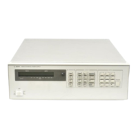
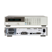
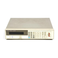
1-3 INSTRUMENT AND MANUAL
IDENTIFICATION ..……………….…………….........1-1
1-4 FIRMWARE REVISIONS…...……...............................1-2
Section II
PRINCIPLES OF OPERATION
2-1 INTRODUCTION .………........................................... 2-1
2-2 OVERALL BLOCK DIAGRAM DESCRIPTION
(Figure 2-1) …..………………………………………..2-1
2-3 AC Input Circuits …………….....................................2-1
2-5 Front Panel …………………………………………….2-1
2-6 Output Board ………………………………………….2-1
2-7
2-9 System MicroComputer ...……………………………2-4
2-16 Output Boards Interface .……..................................... 2-4
2-20 Front Panel Interface ……........................................…2-5
2-23 Bias Supply and Start Up ……....................................2-5
2-24 OUTPUT BOARD ......................................………..…2-7
2-25 Secondary Interface Circuits
(Figure 2-4) ……………………………………………2-7
2-34 Power Mesh and Control Circuits
(Figure 2-5) ……………………………………......…. 2-10
Section III
VERIFICATION
3-1 INTRODUCTION …………......................................... 3-1
3-2 TEST EQUIPMENT REQUIRED …………………….3-1
3-3 OPERATION VERIFICATION TESTS……............... 3-1
3-4 PERFORMANCE TESTS ...............................………....3-1
3-5 Introduction .................................................…………..3-1
3-6 Measurement Techniques ……………………………3-1
3-10 Constant Voltage (CV) Tests …….............................. 3-4
3-21 Constant Current (CC) Tests ......………....................3-10
3-29 EXTENDED TESTS ……………..................................3-13
3-30 Output Drift Tests .....................................…………...3-13
3-35 TEMPERATURE COEFFICIENT (TC) TESTS ..…...3-14
3-36 Output Voltage and Readbauk Voltage TC ......…...3-14
3-37 Output Current and Readback Current TC ..……...3-15
3-38 Negative Current Limit (-CC) Readback TC .......…3-15
Section IV
TROUBLESHOOTING
4-1 INTRODUCTION ……………………………………..4-1
4-2 ELECTROSTATIC PROTECTION ………………..…4-1
4-3 REMOVAL AND REPLACEMENT …………………4-2
4-4 Top Cover Removal …………………………………..4-2
4-5 Gaining Access to Assemblies in the Supply …….…4-2
4-6 ………………………………4-2
4-7 40 Watt Output Board Removal……………………...4-2
4-8 80 Watt Output Board Removal……………………...4-4
4-9 Replacing the power Module U338 (U339) …………4-4
4-10 Front Panel Removal ………………………………….4-4
4-11 Chassis Mounted Components ………………………4-5
4-12 TEST EQUIPMENT REQUIRED ..…………………4-5
4-13 FUSE REPLACEMENT …………………………….…4-5
4-14 INITIAL TROUBLESHOOTING AND
BOARD ISOLATION PROCEDURES ……………....4-8
4-15 Power-On Self Test ……………………………………4-8
4-16 Connector P201 Jumper Positions …………………..4-9
4-17 ERROR Codes and Messages ………………………...4-9
4-18
TROUBLESHOOTING PROCEDURES ……………4-13
4-19 Test Setup ……………………………………………..4-13
4-20 Post Repair Calibration ...……................................... 4-13
4-21
(MODEL Command) ..……...................................... 4-13
4-22 Signature Analysis Testing ……….............................4-14
4-23 Test Setup for S.A......................................………….. 4-14
4-24 Firmware Revisions (ROM? Command) ……..........4-14
4-25 OUTPUT BOARD TROUBLESHOOTING
PROCEDURES …………............................................ 4-30
4-26 Test Setup ………….................................................... 4-30
4-27 Post Repair Calibration ……….................................. 4-30
4-28 Self Exercise Routine on the Output Board……......4-30
4-29 Troubleshooting Analog Multiplexer U323 and
Readbadk Using VMUX? Command ....……….......4-49
4-30 Understanding and Troubleshooting the Signal
Processor (U327) …………..........................................4-50
4-34 Miscellaneous Trouble Symptoms
and Remedies ....................................……………......4-54
REPLACEABLE PARTS
5-1 INTRODUCTION ……………………………………..5-1
5-2 HOW TO ORDER PARTS ………………………….5-1
i
V
Section
4-33 Power Module …………...............................4-54 Signal
Setting the Model Number
GPIB Board Removal
2-4 GPIB Board ……….......................................................2-1
GPIB Board (Figure 2-3) …………………………….2-2
2-8 GPIB Interface ….……………………………………2-3
GPIB BOARD AND FRONT PANEL
 Loading...