Chapter 2: Board Components 2–39
Memory
August 2017 Altera Corporation Cyclone V GT FPGA Development Board
Reference Manual
R8
DDR3A_A6
AK17 1.5-V SSTL Class I Address bus
R2
DDR3A_A7
AL17 1.5-V SSTL Class I Address bus
T8
DDR3A_A8
AH16 1.5-V SSTL Class I Address bus
R3
DDR3A_A9
AJ16 1.5-V SSTL Class I Address bus
L7
DDR3A_A10
AL16 1.5-V SSTL Class I Address bus
R7
DDR3A_A11
AM16 1.5-V SSTL Class I Address bus
N7
DDR3A_A12
AM13 1.5-V SSTL Class I Address bus
T3
DDR3A_A13
AN13 1.5-V SSTL Class I Address bus
M2
DDR3A_BA0
AN16 1.5-V SSTL Class I Bank address bus
N8
DDR3A_BA1
AN17 1.5-V SSTL Class I Bank address bus
M3
DDR3A_BA2
AP17 1.5-V SSTL Class I Bank address bus
K3
DDR3A_CASN
AP15 1.5-V SSTL Class I Row address select
K9
DDR3A_CKE
AP26 1.5-V SSTL Class I Column address select
J7
DDR3A_CLK_P
AA18
Differential 1.5-V SSTL
Class I
Differential output clock
K7
DDR3A_CLK_N
AA17
Differential 1.5-V SSTL
Class I
Differential output clock
L2
DDR3A_CSN
AA16 1.5-V SSTL Class I Chip select
E7
DDR3A_DM0
AL21 1.5-V SSTL Class I Write mask byte lane
D3
DDR3A_DM1
AM24 1.5-V SSTL Class I Write mask byte lane
E3
DDR3A_DQ0
AN19 1.5-V SSTL Class I Data bus byte lane 0
F7
DDR3A_DQ1
AM19 1.5-V SSTL Class I Data bus byte lane 0
F2
DDR3A_DQ2
AP20 1.5-V SSTL Class I Data bus byte lane 0
F8
DDR3A_DQ3
AP21 1.5-V SSTL Class I Data bus byte lane 0
H3
DDR3A_DQ4
AH19 1.5-V SSTL Class I Data bus byte lane 0
H8
DDR3A_DQ5
AG19 1.5-V SSTL Class I Data bus byte lane 0
G2
DDR3A_DQ6
AJ19 1.5-V SSTL Class I Data bus byte lane 0
H7
DDR3A_DQ7
AM21 1.5-V SSTL Class I Data bus byte lane 0
D7
DDR3A_DQ8
AM20 1.5-V SSTL Class I Data bus byte lane 1
C3
DDR3A_DQ9
AL20 1.5-V SSTL Class I Data bus byte lane 1
C8
DDR3A_DQ10
AN22 1.5-V SSTL Class I Data bus byte lane 1
C2
DDR3A_DQ11
AN23 1.5-V SSTL Class I Data bus byte lane 1
A7
DDR3A_DQ12
AP24 1.5-V SSTL Class I Data bus byte lane 1
A2
DDR3A_DQ13
AP25 1.5-V SSTL Class I Data bus byte lane 1
B8
DDR3A_DQ14
AN26 1.5-V SSTL Class I Data bus byte lane 1
A3
DDR3A_DQ15
AN24 1.5-V SSTL Class I Data bus byte lane 1
F3
DDR3A_DQS_P0
AB19
Differential 1.5-V SSTL
Class I
Data strobe P byte lane 0
G3
DDR3A_DQS_N0
AC19
Differential 1.5-V SSTL
Class I
Data strobe N byte lane 0
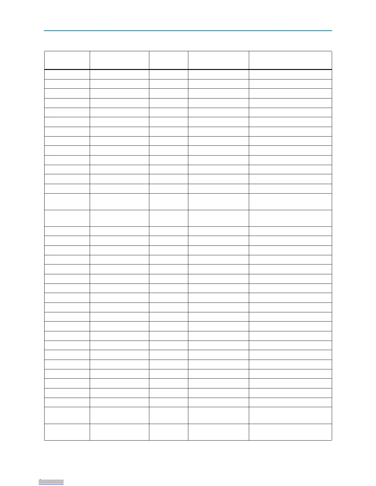
Table 2–28. DDR3A Device Pin Assignments, Schematic Signal Names, and Functions (Part 2 of 5)
Board Reference
Schematic
Signal Name
Cyclone V GT
Pin Number
I/O Standard Description
Downloaded from Arrow.com.Downloaded from Arrow.com.Downloaded from Arrow.com.Downloaded from Arrow.com.Downloaded from Arrow.com.Downloaded from Arrow.com.Downloaded from Arrow.com.Downloaded from Arrow.com.Downloaded from Arrow.com.Downloaded from Arrow.com.Downloaded from Arrow.com.Downloaded from Arrow.com.Downloaded from Arrow.com.Downloaded from Arrow.com.Downloaded from Arrow.com.Downloaded from Arrow.com.Downloaded from Arrow.com.Downloaded from Arrow.com.Downloaded from Arrow.com.Downloaded from Arrow.com.Downloaded from Arrow.com.Downloaded from Arrow.com.Downloaded from Arrow.com.Downloaded from Arrow.com.Downloaded from Arrow.com.Downloaded from Arrow.com.Downloaded from Arrow.com.Downloaded from Arrow.com.Downloaded from Arrow.com.Downloaded from Arrow.com.Downloaded from Arrow.com.Downloaded from Arrow.com.Downloaded from Arrow.com.Downloaded from Arrow.com.Downloaded from Arrow.com.Downloaded from Arrow.com.Downloaded from Arrow.com.Downloaded from Arrow.com.Downloaded from Arrow.com.Downloaded from Arrow.com.Downloaded from Arrow.com.Downloaded from Arrow.com.Downloaded from Arrow.com.Downloaded from Arrow.com.Downloaded from Arrow.com.Downloaded from Arrow.com.Downloaded from Arrow.com.
 Loading...


