Chapter 2: Board Components 2–41
Memory
August 2017 Altera Corporation Cyclone V GT FPGA Development Board
Reference Manual
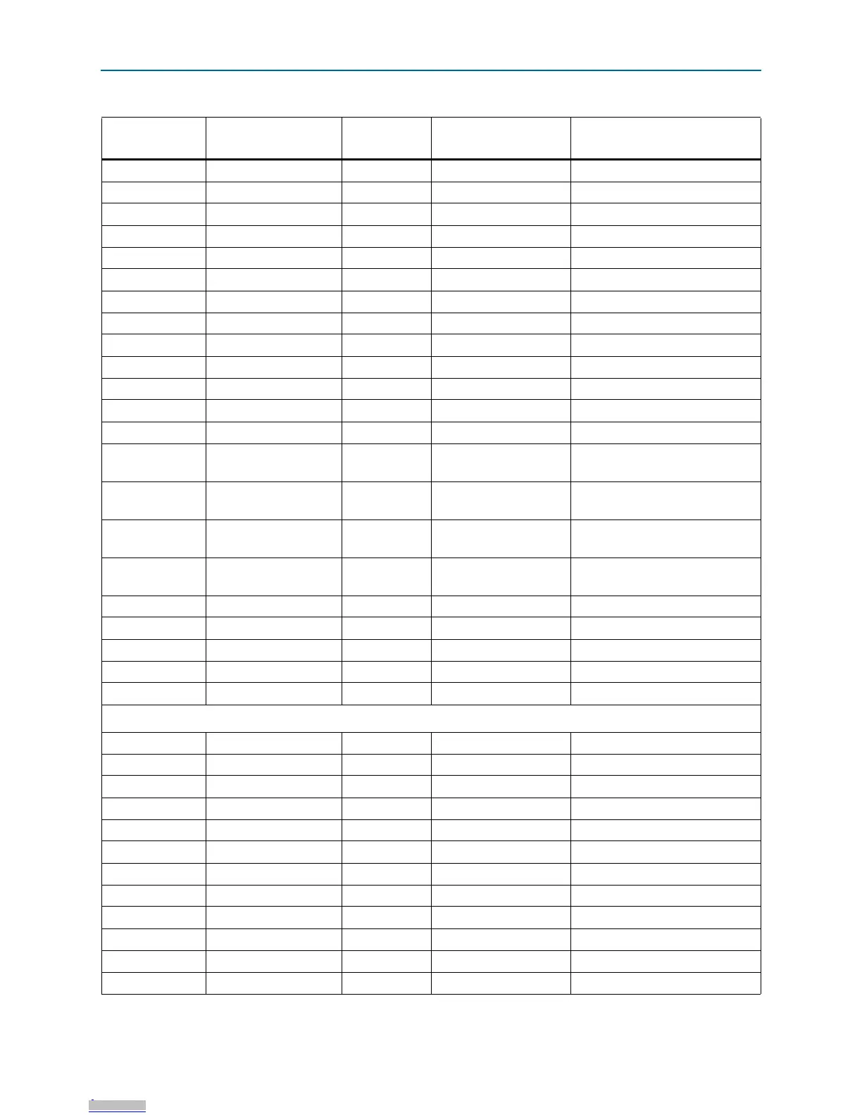
F8
DDR3A_DQ19
AJ21 1.5-V SSTL Class I Data bus byte lane 2
H3
DDR3A_DQ20
AH21 1.5-V SSTL Class I Data bus byte lane 2
H8
DDR3A_DQ21
AH22 1.5-V SSTL Class I Data bus byte lane 2
G2
DDR3A_DQ22
AP30 1.5-V SSTL Class I Data bus byte lane 2
H7
DDR3A_DQ23
AN28 1.5-V SSTL Class I Data bus byte lane 2
D7
DDR3A_DQ24
AL23 1.5-V SSTL Class I Data bus byte lane 3
C3
DDR3A_DQ25
AK23 1.5-V SSTL Class I Data bus byte lane 3
C8
DDR3A_DQ26
AL25 1.5-V SSTL Class I Data bus byte lane 3
C2
DDR3A_DQ27
AM26 1.5-V SSTL Class I Data bus byte lane 3
A7
DDR3A_DQ28
AK24 1.5-V SSTL Class I Data bus byte lane 3
A2
DDR3A_DQ29
AJ24 1.5-V SSTL Class I Data bus byte lane 3
B8
DDR3A_DQ30
AN31 1.5-V SSTL Class I Data bus byte lane 3
A3
DDR3A_DQ31
AL28 1.5-V SSTL Class I Data bus byte lane 3
F3
DDR3A_DQS_P2
AJ20
Differential 1.5-V SSTL
Class I
Data strobe P byte lane 2
G3
DDR3A_DQS_N2
AK20
Differential 1.5-V SSTL
Class I
Data strobe N byte lane 2
C7
DDR3A_DQS_P3
Y20
Differential 1.5-V SSTL
Class I
Data strobe P byte lane 3
B7
DDR3A_DQS_N3
AA20
Differential 1.5-V SSTL
Class I
Data strobe N byte lane 3
K1
DDR3A_ODT
AN21 1.5-V SSTL Class I On-die termination enable
J3
DDR3A_RASN
AP14 1.5-V SSTL Class I Row address select
T2
DDR3A_RESETN
AJ22 1.5-V SSTL Class I Reset
L3
DDR3A_WEN
AN12 1.5-V SSTL Class I Write enable
L8
DDR3A_ZQ2
— 1.5-V SSTL Class I ZQ impedance calibration
DDR3 x16 (U28)
N3
DDR3A_A0
AK18 1.5-V SSTL Class I Address bus
P7
DDR3A_A1
AL18 1.5-V SSTL Class I Address bus
P3
DDR3A_A2
AM18 1.5-V SSTL Class I Address bus
N2
DDR3A_A3
AN18 1.5-V SSTL Class I Address bus
P8
DDR3A_A4
AH17 1.5-V SSTL Class I Address bus
P2
DDR3A_A5
AJ17 1.5-V SSTL Class I Address bus
R8
DDR3A_A6
AK17 1.5-V SSTL Class I Address bus
R2
DDR3A_A7
AL17 1.5-V SSTL Class I Address bus
T8
DDR3A_A8
AH16 1.5-V SSTL Class I Address bus
R3
DDR3A_A9
AJ16 1.5-V SSTL Class I Address bus
L7
DDR3A_A10
AL16 1.5-V SSTL Class I Address bus
R7
DDR3A_A11
AM16 1.5-V SSTL Class I Address bus
Table 2–28. DDR3A Device Pin Assignments, Schematic Signal Names, and Functions (Part 4 of 5)
Board Reference
Schematic
Signal Name
Cyclone V GT
Pin Number
I/O Standard Description
Downloaded from Arrow.com.Downloaded from Arrow.com.Downloaded from Arrow.com.Downloaded from Arrow.com.Downloaded from Arrow.com.Downloaded from Arrow.com.Downloaded from Arrow.com.Downloaded from Arrow.com.Downloaded from Arrow.com.Downloaded from Arrow.com.Downloaded from Arrow.com.Downloaded from Arrow.com.Downloaded from Arrow.com.Downloaded from Arrow.com.Downloaded from Arrow.com.Downloaded from Arrow.com.Downloaded from Arrow.com.Downloaded from Arrow.com.Downloaded from Arrow.com.Downloaded from Arrow.com.Downloaded from Arrow.com.Downloaded from Arrow.com.Downloaded from Arrow.com.Downloaded from Arrow.com.Downloaded from Arrow.com.Downloaded from Arrow.com.Downloaded from Arrow.com.Downloaded from Arrow.com.Downloaded from Arrow.com.Downloaded from Arrow.com.Downloaded from Arrow.com.Downloaded from Arrow.com.Downloaded from Arrow.com.Downloaded from Arrow.com.Downloaded from Arrow.com.Downloaded from Arrow.com.Downloaded from Arrow.com.Downloaded from Arrow.com.Downloaded from Arrow.com.Downloaded from Arrow.com.Downloaded from Arrow.com.Downloaded from Arrow.com.Downloaded from Arrow.com.Downloaded from Arrow.com.Downloaded from Arrow.com.Downloaded from Arrow.com.Downloaded from Arrow.com.Downloaded from Arrow.com.Downloaded from Arrow.com.
 Loading...


