6
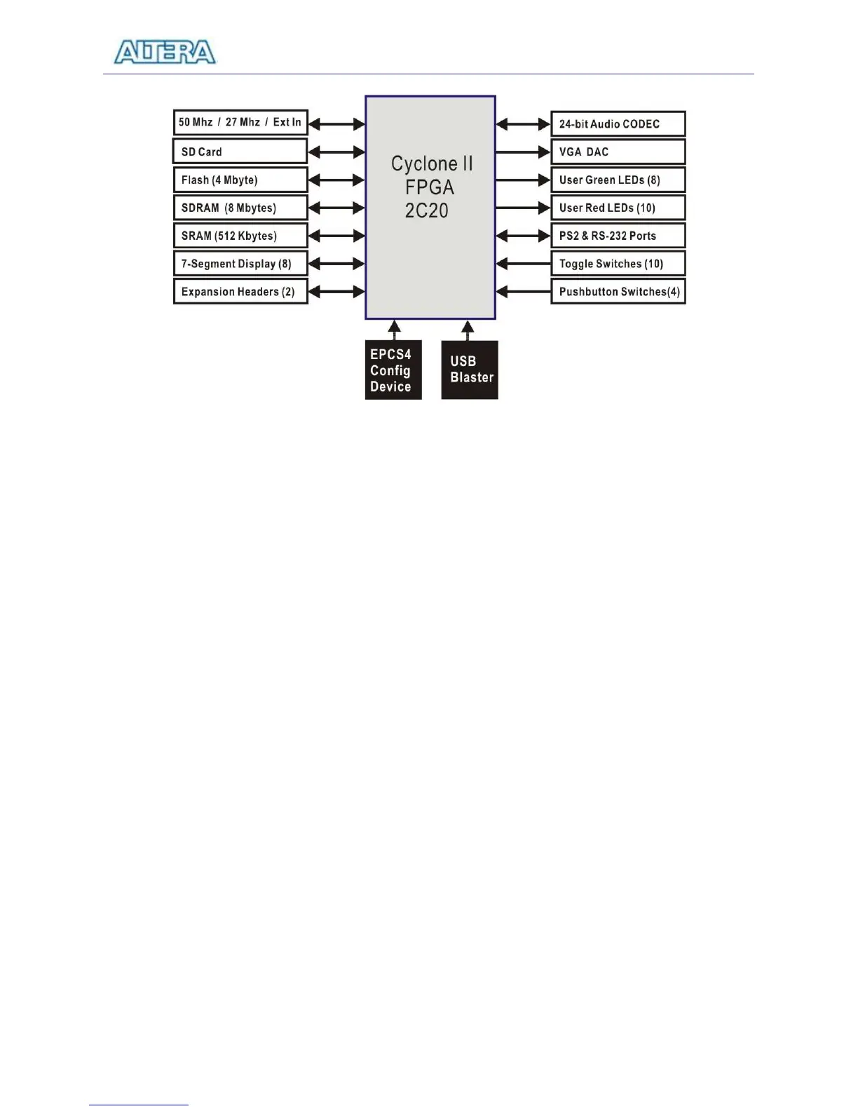
Figure 2.2. Block diagram of the DE1 board.
Following is more detailed information about the blocks in Figure 2.2:
Cyclone II 2C35 FPGA
• 18,752 LEs
• 52 M4K RAM blocks
• 240K total RAM bits
• 26 embedded multipliers
• 4 PLLs
• 315 user I/O pins
• FineLine BGA 484-pin package
Serial Configuration device and USB Blaster circuit
• Altera’s EPCS4 Serial Configuration device
• On-board USB Blaster for programming and user API control
• JTAG and AS programming modes are supported
SRAM
• 512-Kbyte Static RAM memory chip
• Organized as 256K x 16 bits
• Accessible as memory for the Nios II processor and by the DE1 Control Panel
SDRAM