32
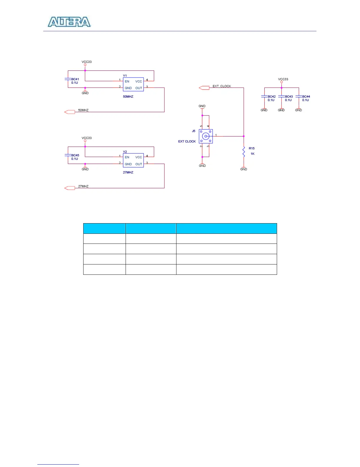
Figure 4.8. Schematic diagram of the clock circuit.
Signal Name FPGA Pin No. Description
CLOCK_27 PIN_D12, PIN_E12 27 MHz clock input
CLOCK_50 PIN_L1 50 MHz clock input
CLOCK_24 PIN_A12, PIN_B12 24 MHz clock input from USB Blaster
EXT_CLOCK PIN_M21 External (SMA) clock input
Table 4.5. Pin assignments for the clock inputs.
4.5 Using the Expansion Header
The DE1 Board provides two 40-pin expansion headers. Each header connects directly to 36 pins on
the Cyclone II FPGA, and also provides DC +5V (VCC5), DC +3.3V (VCC33), and two GND pins.
Figure 4.10 shows the related schematics. Each pin on the expansion headers is connected to two
diodes and a resistor that provide protection from high and low voltages. The figure shows the
protection circuitry for only four of the pins on each header, but this circuitry is included for all 72
data pins. Table 4.7 gives the pin assignments.