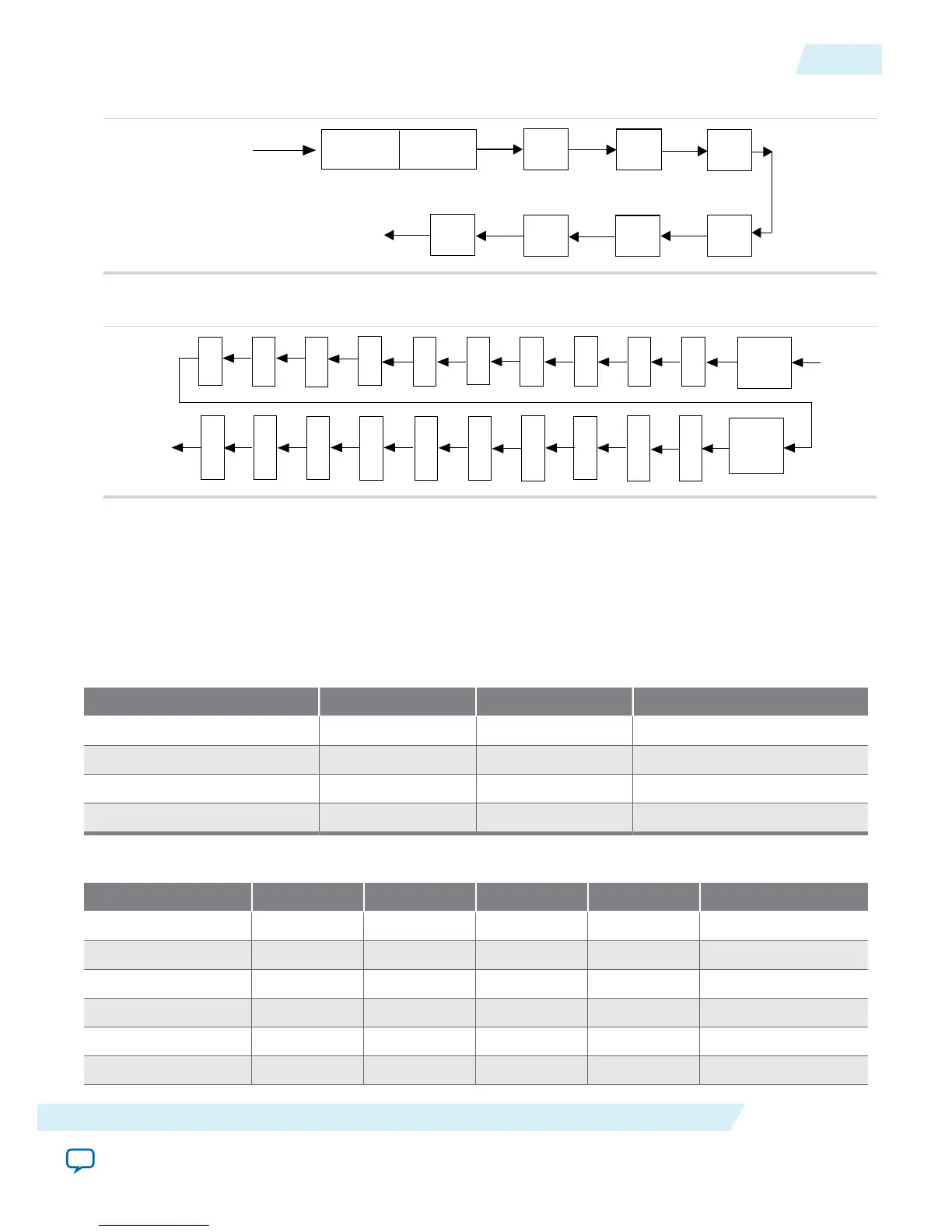
Figure 4-7: PLL Component Scan Chain Order
DATAIN
C1C2C3C4
DATAOUT
MSB
LF CP
LSB
N M C0
Figure 4-8: PLL Post-Scale Counter Scan Chain Bit Order
DATAIN
rbypass
HB
7
HB
6
HB
5
HB
4
HB
3
HB
2
HB
1
HB
0
rselodd
LB
7
LB
6
LB
5
LB
4
LB
3
LB
2
LB
1
LB
0
DATAOUT
HB
9
HB
8
LB
9
LB
8
Charge Pump and Loop Filter
You can reconfigure the following settings to update the PLL bandwidth in real time:
• Charge pump (I
CP
)
• Loop filter resistor (R)
• Loop filter capacitor (C)
Table 4-2: Charge Pump Bit Control
CP[2] CP[1] CP[0] Setting (Decimal)
0 0 0 0
0 0 1 1
0 1 1 3
1 1 1 7
Table 4-3: Loop Filter Resistor Value Control
LFR[4] LFR[3] LFR[2] LFR[1] LFR[0] Setting (Decimal)
0 0 0 0 0 0
0 0 0 1 1 3
0 0 1 0 0 4
0 1 0 0 0 8
1 0 0 0 0 16
1 0 0 1 1 19
UG-M10CLKPLL
2015.06.12
Charge Pump and Loop Filter
4-13
MAX 10 Clocking and PLL Implementation Guides
Altera Corporation
Send Feedback