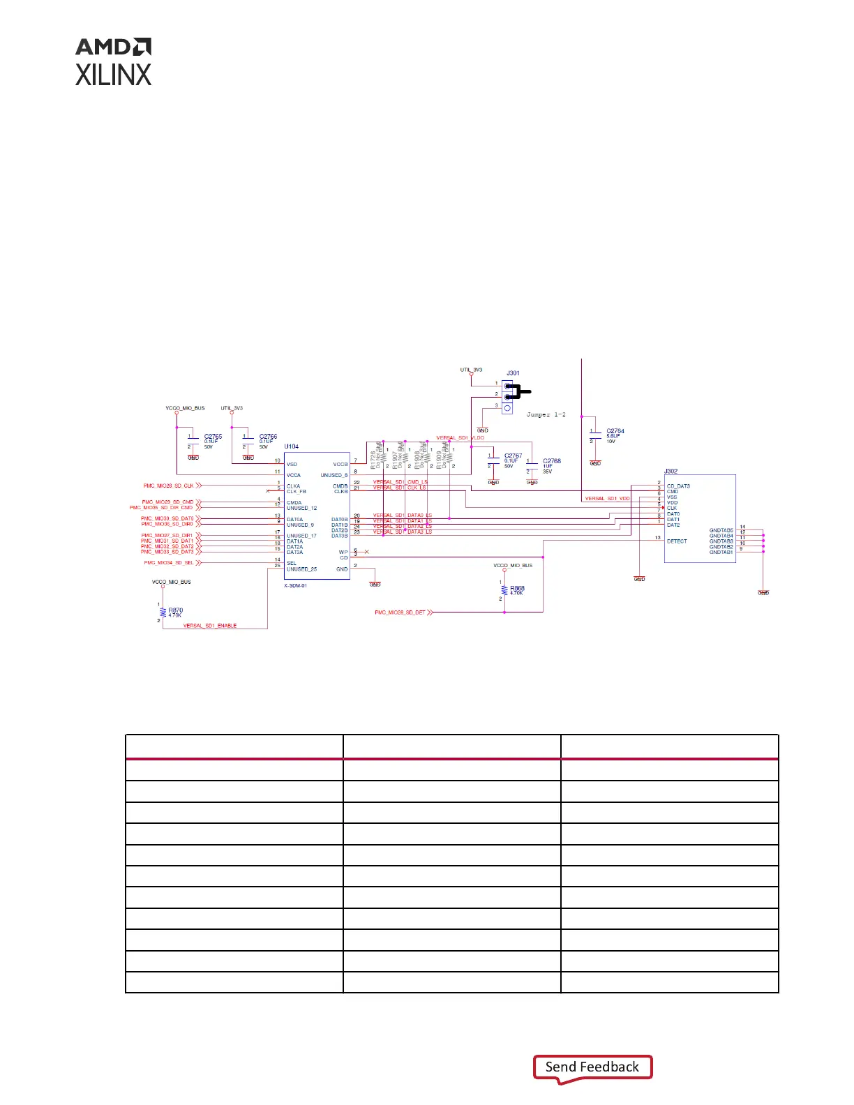
The VPK180 evaluaon board includes a secure digital input/output (SDIO) interface to provide
access to general purpose non-volale SDIO memory cards and peripherals. This interface is
used for the SD boot mode and supports SD2.0 and SD3.0 access.
The SDIO interface signals PMC_MIO[26:36, 51] are connected to XCVP1802 ACAP bank 501,
which has its VCCO set to 1.8V. Six SD interface nets PMC_MIO[26, 29, 30:33] are passed
through a NXP NVT4857UK SD 3.0-compliant voltage level-translator U104. This translator is
present between the Versal ACAP and the SD card connector (J302). The NXP NVT4857UK
U104 device provides SD3.0 capability with SDR104 performance. The following gure shows
the connecons of the SD card interface on the VPK180 evaluaon board.
Figure 10: SD Card Interface Connections
X26058-120921
The following table lists the NVT4857UK U104 adapter pinout.
Table 8: NVT4857UK U104 Adapter Pinout
Aries Adapter Pin Number NVT4857UKAZ Pin Number NVT4857UKAZ Pin Name
1 D2 CLKA
2 C3, C2 GND
3 B2 CD
4 C1 CMDA
5 E2 CLK_FB
6 Unused Unused
7 B3 VCCB
8 Unused Unused
9 Unused Unused
10 A3 VSD
11 A2 VCCA
Chapter 3: Board Component Descriptions
UG1582 (v1.0) February 21, 2023 www.xilinx.com
VPK180 Board User Guide 35