AN-877 Application Note
Rev. B | Page 10 of 20
05739-010
SLAVE SPI
MEMORY
ENCODE
CLOCK
0x0FF
BIT 0
0
1
OPTIONAL
EXTERNAL
SYNC
MASTER SPI
MEMORY
0x0FF
BIT 7
BIT 0
RESET
Q
Q
SET
CLR
D
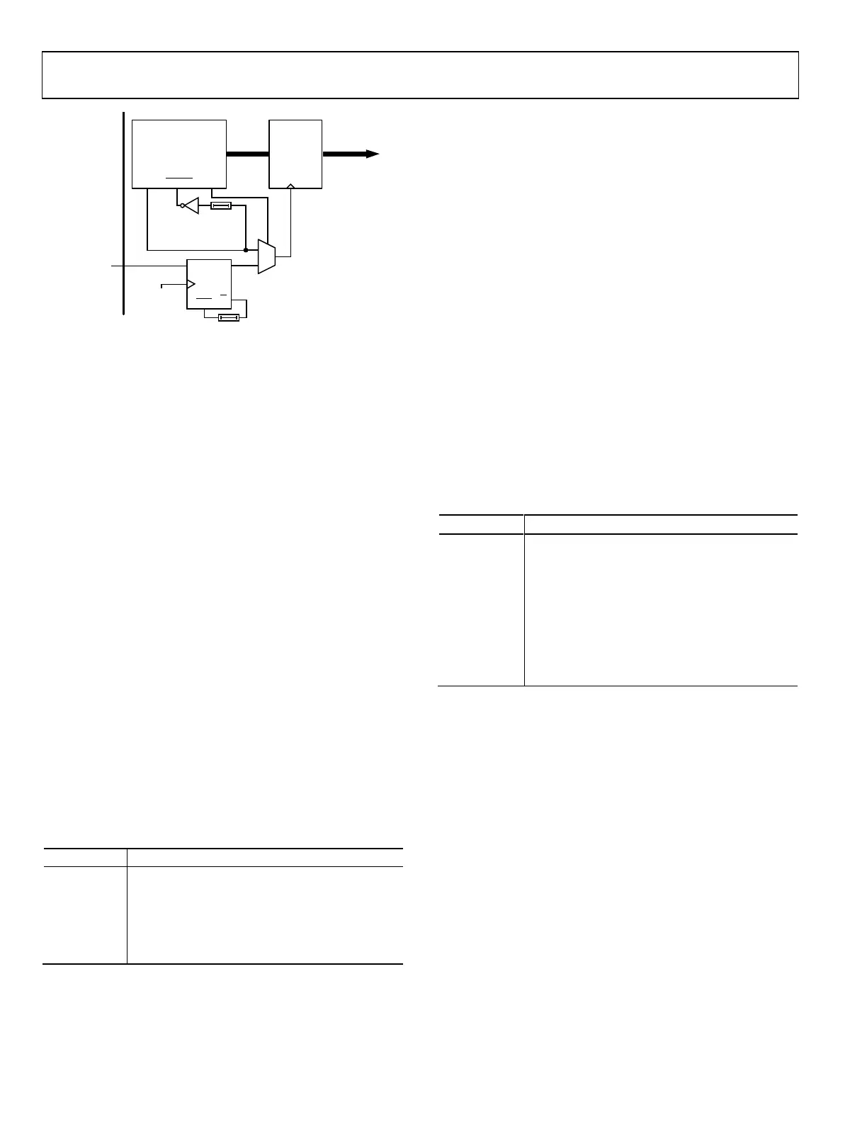
Figure 13. Internal Latching Flow
PROGRAM REGISTERS
Program registers may or may not be indexed by Register 0x004
and Register 0x005 (see the device data sheet to determine how
the device uses these registers).
Modes (0x008)
Register 0x008 controls the mode of the chip.
Bit 7—External Power-Down Enable
Bit 7 enables use of an external power-down pin, if available
(see the individual device data sheet to determine if this pin is
provided). If this bit is clear, any register-based power settings
(Bit 0 through Bit 2) take priority. However, if this bit is set, the
external pin determines the operating mode of the chip, in
conjunction with Bit 6 and Bit 5. If Bit 7 is high and the external
pin is low, the chip mode is determined by Bits[6:5]. If Bit 7 is
high and the external pin is high, the chip is placed in normal
operating mode, as defined by other device settings. If no external
power-down pin is provided, Bit 7 to Bit 5 are ignored.
Bit 6 to Bit 5—External Power-Down Mode
If Bit 6 to Bit 5 are set to:
• 00, full power-down results when the external pin is active.
• 01, a standby state results when the external pin is active.
• 10, this indicates a reserved mode.
• 11, the digital output is enabled when the external pin is
active.
Table 4. External Pin Modes, Register 0x008, Bits[6:5]
Bit 6 to Bit 5 Mode Description of External Pin Control
00
Enter full power-down when external pin is
active
01 Enter chip standby when external pin is active
10 Reserved
11
Enable digital outputs when external pin is
active (low)
Bit 4—Reserved
Bit 3—Function Bypass
When Bit 3 is set, on-chip analog signal processing blocks are
bypassed and powered down (see the device data sheet for
specific details).
Bit 2 to Bit 0—Internal Power-Down Mode
Bit 2 to Bit 0 determine the mode of chip operation.
The following settings are available for these bits:
• 000 is normal chip operation.
• 001 is a full chip power-down of both analog and clock
circuitry, that is, low power sleep mode.
• 010 shuts the chip down, but allows for a rapid restart.
• 011 is chip reset.
• 100 shuts down the core ADC of devices that include an
analog signal processing block or an analog front end
(AFE).
• 101 shuts down the AFE of devices that include analog
signal processing blocks of an AFE.
• 110 through 111 are reserved for future operating modes.
Table 5. Power Modes, Register 0x008, Bits[2:0]
Bit 2 to Bit 0 Chip Power Mode Description
000 Chip run (default)
001 Full power-down
010 Standby mode
011
Chip reset (after reset, the device defaults back
to chip run—same as 000)
100 ADC power-down (for chips with an AFE)
101 AFE power-down (for chips with an AFE)
110 Reserved
111 Reserved
Clock (0x009)
Register 0x009 is used to configure the chip clocking.
Bit 7 to Bit 3—Reserved
Bit 2—Phase-Locked Loops (PLL) Enable
Setting this bit enables any on-chip PLL.
Bit 1—Clock Boost
Bit 1 is used to enhance the performance of the clock function.
Setting this bit increases current levels in the clock circuit to
improve clock jitter performance. Clearing this bit reduces
power, but increases the jitter of the clock circuit (see the device
data sheet for additional details).
Bit 0—Duty Cycle Stabilizer
Bit 0 is used to disable or enable the internal duty cycle
stabilizer (DCS). If Bit 0 is set, then the DCS is enabled. The
default for this register is 0x01, which enables the DCS.
 Loading...