AN-877 Application Note
Rev. B | Page 18 of 20
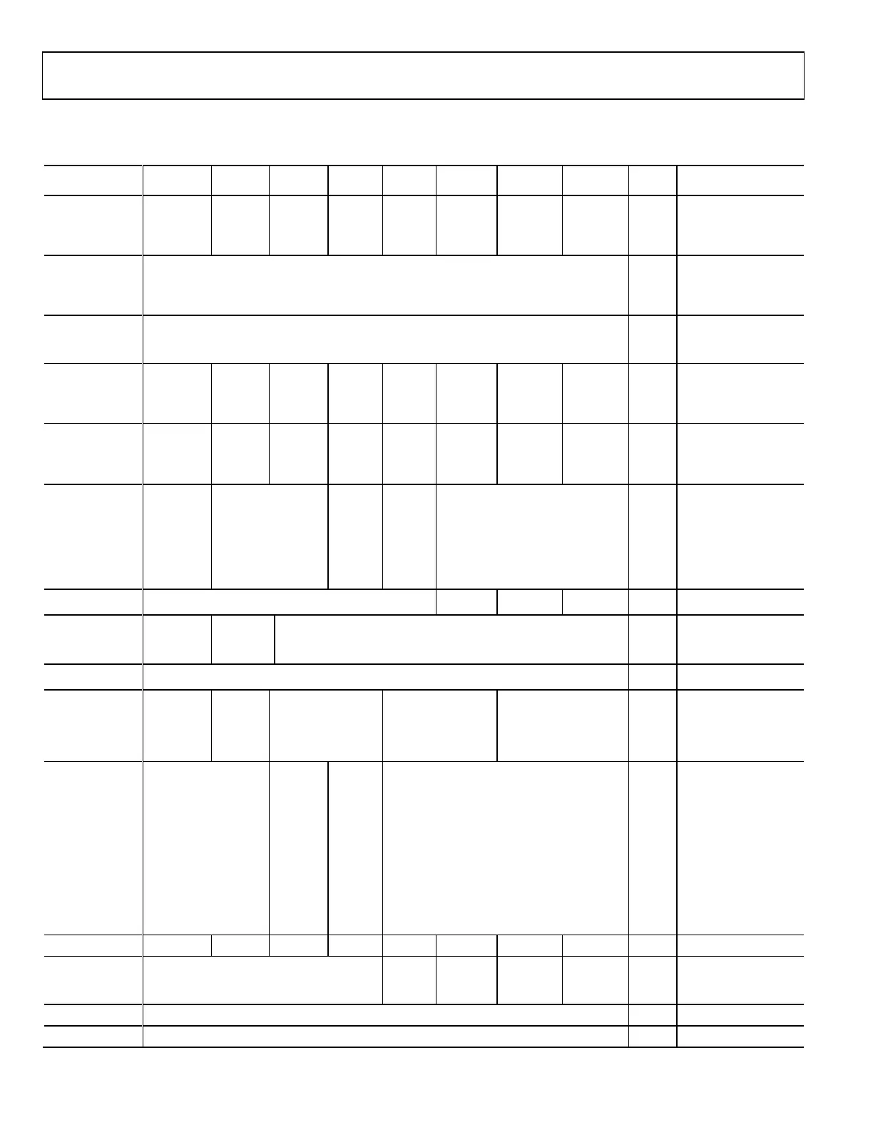
CONTROL REGISTER
Table 14. Control Register Map
Address
1
, Register Bit 7 (MSB) Bit 6 Bit 5 Bit 4 Bit 3 Bit 2 Bit 1 Bit 0 (LSB)
Default
Value
1
Comments
00,
CHIP_PORT_CONFIG
SDO active
2
LSB first Soft reset
Should
be set.
Do not
clear.
18h
The nibbles should be
mirrored by the user so
that LSB-first or MSB-first
mode registers correctly
regardless of shift mode.
01, CHIP_ID 8-bit chip ID; Bits[7:0]
Read
only
Default is unique chip ID,
different for each device.
This is a read-only register.
(See device data sheet for
more details.)
02, CHIP_GRADE 8-bit child ID
Read
only
Read only. Child ID used
to differentiate graded
devices. (See device data
sheet for more details.)
04,
DEVICE_INDEX_B
AUX 7 AUX 6 AUX 5 AUX 4 ADC 7 ADC 6 ADC 5 ADC 4 FFh
Bits are set to determine
which device on -chip
receives the next write
command. The default will
be all devices on-chip.
DEVICE_INDEX_A
AUX 3 AUX 2 AUX 1 AUX 0 ADC 3 ADC 2 ADC 1 ADC 0 FFh
Bits are set to determine
which device on-chip
receives the next write
command. The default is
all devices on-chip.
08, MODES
power-down
enable
mode
00: full power-down
01: standby
10: normal mode
(output disabled)
11: normal mode
(output enabled)
bypass
0: chip run
1: full power-down
2: standby
3: reset
4: ADC power-down
5: analog front-end power-down
6: reserved
7: reserved
00h
generic modes of chip
operation.
09, CLOCK Reserved for additional clock input support PLL enable Clock boost
Duty cycle
stabilize
01h
0A, PLL_CONTROL PLL locked PLL auto PLL multiplier; Bits[5:0] 00h
Configures on-chip PLL by
enabling and setting
multiplier. MSB is set
when the PLL is locked.
0B, CLOCK_DIVIDE Clock divider; Bits[7:0] 00h
The divide ratio is the
value plus 1.
0C, ENHANCE Reserved Reserved Reserved
Chop enable
0: off
1: Mode 1
2: Reserved
3: Reserved
Shuffle mode
0: off
1: Mode 1
2: Reserved
3: Reserved
Shuffle mode determines
how shuffling is
performed. Chopping
determines how the input
is processed to improve
noise near dc.
0D, TEST_IO
User test mode
00: single
01: alternate
10: single once
11: alternate once
Reset PN
long gen
Reset PN
short gen
Output test mode
0: off
1: midscale short
2: +FS short
3: −FS short
4: checkerboard output
5: PN23 sequence
6: PN9
7: 1/0 word toggle
8: User input
9: 1/0 bit toggle
10: 1× sync
11: 1 bit high
12: mixed-bit frequency (format
determined by OUTPUT_MODE)
00h
When set, the test data is
placed on the output pins
in place of normal data.
0E, TEST_ BIST BIST init Reserved BIST e nable 00h BIST mode configuration
0F, ADC_INPUT
Low-pass filter bandwidth
0: default
Bits[1:15]: alternate corner frequencies
(See device data sheet for details)
Analog
disconnect
Common-
mode
input
enable
Single
ended
00h
10, OFFSET 8-bit device offset adjustment; Bits[7:0] 80h Device offset trim
11, GAIN 8-bit device gain adjustment; Bits[7:0] 00h Device gain trim
 Loading...