AN-877 Application Note
Rev. B | Page 4 of 20
SERIAL DATA OUT (SDO)
To determine if a device supports the SDO pin, refer to the device
data sheet. If SDO is present, it is in a high impedance state, unless
data is actively being shifted on this pin to allow tying multiple
devices together at the receiving end. Additionally, data is shifted
out on the first falling edge of SCLK after the instruction phase is
complete. When data is returned to the controller, the information
is placed in the output shifters, within the time period between the
last rising edge of SCLK associated with the instruction phase and
the immediately next falling edge. This can be nominally 20 ns
when operating at 25 MHz.
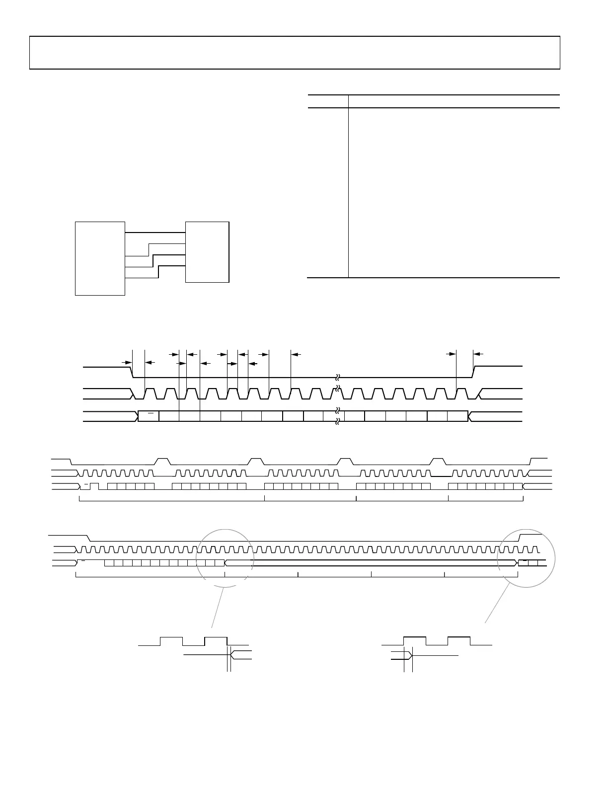
CSB
SCLK
SCLK
SDO
SDO
SDI
SDIO
CSB
SPI
CONTROLLER
CONVERTER
INTERFACE
HIGH-Z WHEN
NOT USED OR
INACTIVE
05739-002
Figure 3. 3-Wire Control
Table 1. Serial Timing Specifications
1
Symbol Description
t
DS
Setup time between data and rising edge of SCLK.
t
DH
Hold time between data and rising edge of SCLK.
t
CLK
Period of the clock.
t
S
Setup time between CSB and SCLK.
t
H
Hold time between CSB and SCLK.
t
HI
Minimum period that SCLK needs to be in a logic
high state.
t
LO
Minimum period that SCLK needs to be in a logic
low state.
t
EN_ SDI O
Minimum time it takes the SDIO pin to switch
between an input and an output relative to SCLK
falling edge.
t
DIS_ SDI O
Minimum time it takes the SDIO pin to switch
between an output and an input, relative to SCLK
rising edge.
1
See device data sheet for minimum and maximum ratings.
t
S
t
DS
t
DH
t
HI
t
LO
t
CLK
t
H
DON'T CARE
DON'T CARE
W1 W0 A12 A11 A10 A9 A8
A7 D5 D4 D3 D2 D1 D0
DON'T CARE
DON'T CARE
CSB
Figure 4. Setup and Hold Timing Measurements
CSB
SCLK
SDIO
DON'T CARE
W0
A12
A11 A10 A9 A8
A7 A6 A5 A4 A3 A2 A1 A0
R/W W1
DON'T CARE
DON'T CARE
16-BIT INSTRUCTION HEADER
MSB-FIRST 16-BIT INSTRUCTION, 3 BYTES DATA WITH STALLING
REGISTER (N) DATA
REGISTER (N–1) DATA
REGISTER (N–2) DATA
D6 D5 D4 D3 D2 D1 D0D7
DON'T CARE
D6 D5 D4 D3 D2 D1 D0D7
D6 D5 D4 D3 D2 D1 D0D7
05739-011
Figure 5. Most Significant Bit (MSB)-First Instruction and Data with Stalling
SDIO
DON'T CARE
W0
A11
A11 A10 A9 A8 A7 A6 A5 A4 A3 A2 A1 A0R/W W1
. . .
DON'T CARE
16-BIT INSTRUCTION HEADER
REGISTER (N – 1) DATA
REGISTER (N – 2) DATA
OUTPUT DRIVER OFF
R/W W1
DRIVEN OUTPUT DATA STREAM
t
EN_SDIO
t
DIS_SDIO
OUTPUT DRIVER ON
MSB FIRST 16-BIT READ INSTRUCTION, 4 BYTES DATA 4-WIRE
REGISTER (N) DATA REGISTER (N – 3) DATA
OUTPUT DRIVER ON OUTPUT DRIVER OFF
Figure 6. Typical SDIO Output Enable and Disable Timing
 Loading...