Application Note AN-877
Rev. B | Page 7 of 20
DETECTION OF SPI MODE AND PIN MODE
Some users may choose not to use an SPI port to configure their
device. Where possible, devices are designed to power up using
typical settings. (For exact details, consult the appropriate de vice
data sheet.) However, there may be cases where users want to
change the basic features without inclusion of an SPI controller.
Examples include controlling the duty cycle stabilizer or the
format of the data output between twos complement and offset
binary. For these types of options, the chip can be specified such
that external controls can be used to change the options without
having to program the device. To minimize the number of
external pins, the SPI pins are reassigned to these alternate
functions.
For devices that implement this option (see the device data sheet to
determine if this option is supported), the user can choose to
enable the pin control modes. To do so, the CSB line must be
tied high. While this pin is high, the remaining SPI pins become
alternate functions, and any setting on those pins takes effect as
defined in the device data sheet. Once the user decides to enter
SPI mode, pin mode cannot be re-entered unless the device is
powered off first.
At power up, the device defaults to pin control mode as long as
CSB is logic high. If the CSB line is wired high, the device always
functions in pin control mode. Likewise, if the CSB line is wired
low, the device powers up in SPI mode (see the Stream ing section
for limitations in this mode). In most cases, the CSB line is used
to select the chip. Typically, in this mode, CSB is taken high usually
at power up by the external SPI controller. Therefore, by default,
the remaining SPI pins initially function in pin control mode. As
soon as the CSB line is taken low to select the chip, the SPI function
is enabled, which ignores the state of the other pins and places
control strictly with the settings of the internal memory map.
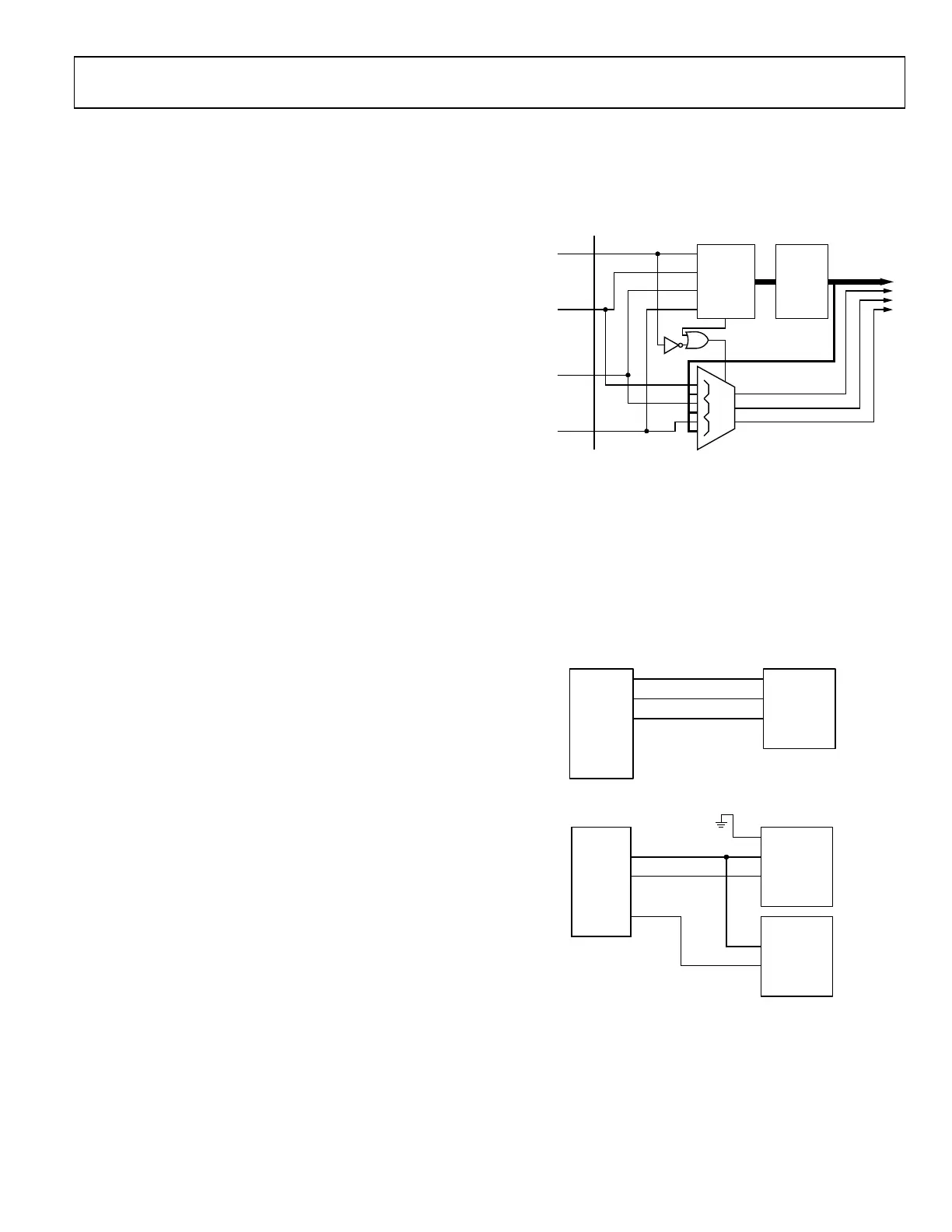
When the CSB line is low, the state machine expects an SCLK to
shift in data. After 9 clock cycles, representing the first byte (plus an
extra cycle), the internal state machine no longer looks at the
CSB pin to determine if pin mode or SPI mode is used. The logic
used for this is shown in Figure 9. As long as the CSB line is high
from power-up, an internal mux is used to select the alternate
functions for the SPI pins. Once the CSB line is taken low, the
mux is deselected from the input pins and begins interpreting
these signals as SPI signals. After an SPI command is recognized,
the mux stays in the SPI position, regardless of the state of the
CSB line. Therefore, users cannot hop between SPI mode and
pin mode.
Additionally, if the SPI port is being used for control, it is
recommended that the device be configured as part of other
start-up procedures to ensure that the device is ready in the
desired state if the pin mode is not to be used. Performing a soft
rese t function does not cause the part to revert back to pin mode.
The only means to accomplish this are cycling the power on the
device or asserting the device pin reset, if the part is so equipped.
Note that not all parts include a pin reset. See the device data
sheet for details.
CSB
CSB
SDO
SDIO
SCLK
SLAVE SPI
MEMORY
1 TO 3 CONTROL BITS
0
1
0
1
0
1
0/1
05739-006
SCLK OR
ALT 1
SDIO OR
ALT 2
SDO OPTIONAL
OR ALT 3
PIN
MUX
SPI STATE
MACHINE
HI-Z WHEN
NOT USED
OR INACTIVE
FIRST SPI
INSTRUCTION
Figure 9. Hardware Interfacing
HARDWARE INTERFACING
Although these devices are designed to be interfaced to SPI
controllers, it is not necessary to always use an SPI controller to
set up these devices. Pin mode provides one alternative, but in
cases where more flexibility is desired, it is possible to use either
serial PIC or PROMS microcontrollers, as shown in Figure 10
and Figure 11. For more details on programming these devices
with PIC microcontrollers, see the AN-812 Application Note,
Microcontroller-Based Serial Port Interface (SPI) Boot Circuit.
05739-007
CONVERTER
INTERFACE
CSB
SDIO
SCLK
GP2
GP1
GP0
PIC 12F629
Figure 10. Programming with a Low Cost PIC Microcontroller
05739-008
CSB
SDIO
SCLK
SDO
SCLK
SDIO
SCLK
ENABLE
CONVERTER
INTERFACE
DEVICE 1
CLOCK
CONTROLLER
GENERATOR
SPI SERIAL
PROM
Figure 11. Programming with a Low Cost Serial PROM and
External Clock Source
 Loading...