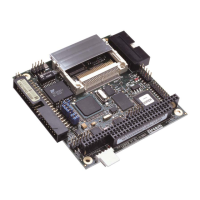
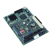
VIPER Detailed hardware description
GPIO
No
AF
Signal Name Dir Active Sleep Function See section…
58 2 LCD_D0 Output NA 0 LCD Data Bit 0
59 2 LCD_D1 Output NA 0 LCD Data Bit 1
60 2 LCD_D2 Output NA 0 LCD Data Bit 2
61 2 LCD_D3 Output NA 0 LCD Data Bit 3
62 2 LCD_D4 Output NA 0 LCD Data Bit 4
63 2 LCD_D5 Output NA 0 LCD Data Bit 5
64 2 LCD_D6 Output NA 0 LCD Data Bit 6
65 2 LCD_D7 Output NA 0 LCD Data Bit 7
66 2 LCD_D8 Output NA 0 LCD Data Bit 8
67 2 LCD_D9 Output NA 0 LCD Data Bit 9
68 2 LCD_D10 Output NA 0 LCD Data Bit 10
69 2 LCD_D11 Output NA 0 LCD Data Bit 11
70 2 LCD_D12 Output NA 0 LCD Data Bit 12
71 2 LCD_D13 Output NA 0 LCD Data Bit 13
72 2 LCD_D14 Output NA 0 LCD Data Bit 14
73 2 LCD_D15 Output NA 0 LCD Data Bit 15
74 2 LCD_FCLK Output NA 0
LCD Frame Clock
(STN)
Vertical Sync (TFT)
75 2 LCD_LCLK Output NA 0
LCD Line Clock
(STN) /
Horizontal Sync (TFT)
76 2 LCD_PCLK Output NA 0
LCD Pixel Clock
(STN) / Clock (TFT)
77 2 LCD_BIAS Output NA 0
LCD Bias (STN) / Date
Enable (TFT)
Flat panel display support
(page 29) and PL3 – LCD
connector
(page 62)
78 2 ETHERCS2 Output Low Hi-Z Chip Select 2
79 2 USBCS Output Low Hi-Z Chip Select 3
80 2 ETHERCS1 Output Low Hi-Z Chip Select 4
VIPER address map
(page
14
)
81 0 SDRAM Input NA Input SDRAM Size
Detection 0 = 64MB,
1 = 16MB
-
82 0 CF_SWITCH Output High 0 CompactFLASH
Power Switch Enable
CompactFLASH (page 24)
and CompactFLASH
power management
(page 57
)
83 0 RTC_IO Bidirec-
tional
NA 0 RTC Data
84 0 RTC_CLK Output 0 RTC Clock
Real Time Clock
(page 21)
© 2004 Arcom Issue H 20