170
8271D–AVR–05/11
ATmega48A/PA/88A/PA/168A/PA/328/P
is requested. The Slave may continue to place new data to be sent into SPDR before reading
the incoming data. The last incoming byte will be kept in the Buffer Register for later use.
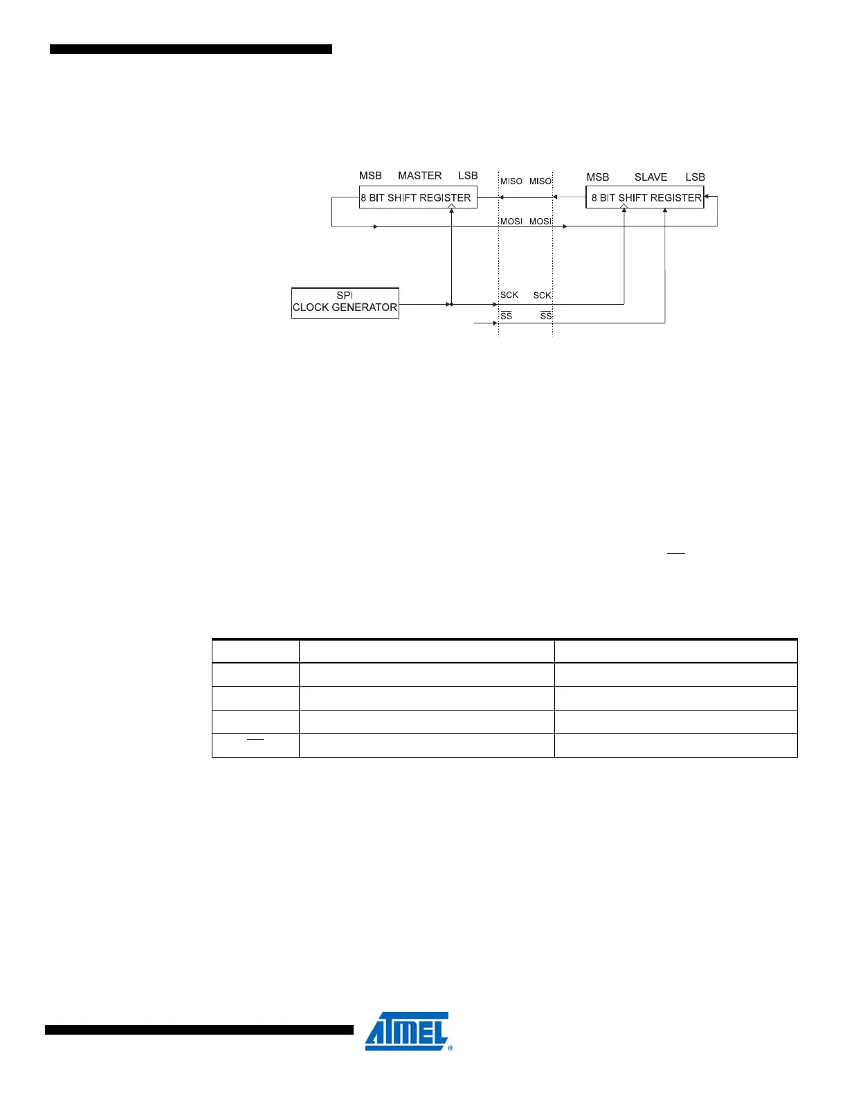
Figure 19-2. SPI Master-slave Interconnection
The system is single buffered in the transmit direction and double buffered in the receive direc-
tion. This means that bytes to be transmitted cannot be written to the SPI Data Register before
the entire shift cycle is completed. When receiving data, however, a received character must be
read from the SPI Data Register before the next character has been completely shifted in. Oth-
erwise, the first byte is lost.
In SPI Slave mode, the control logic will sample the incoming signal of the SCK pin. To ensure
correct sampling of the clock signal, the minimum low and high periods should be:
Low periods: Longer than 2 CPU clock cycles.
High periods: Longer than 2 CPU clock cycles.
When the SPI is enabled, the data direction of the MOSI, MISO, SCK, and SS
pins is overridden
according to Table 19-1 on page 170. For more details on automatic port overrides, refer to
”Alternate Port Functions” on page 82.
Note: See ”Alternate Functions of Port B” on page 84 for a detailed description of how to define the
direction of the user defined SPI pins.
The following code examples show how to initialize the SPI as a Master and how to perform a
simple transmission. DDR_SPI in the examples must be replaced by the actual Data Direction
Register controlling the SPI pins. DD_MOSI, DD_MISO and DD_SCK must be replaced by the
actual data direction bits for these pins. E.g. if MOSI is placed on pin PB5, replace DD_MOSI
with DDB5 and DDR_SPI with DDRB.
Table 19-1. SPI Pin Overrides
(Note:)
Pin Direction, Master SPI Direction, Slave SPI
MOSI User Defined Input
MISO Input User Defined
SCK User Defined Input
SS
User Defined Input