169
8271D–AVR–05/11
ATmega48A/PA/88A/PA/168A/PA/328/P
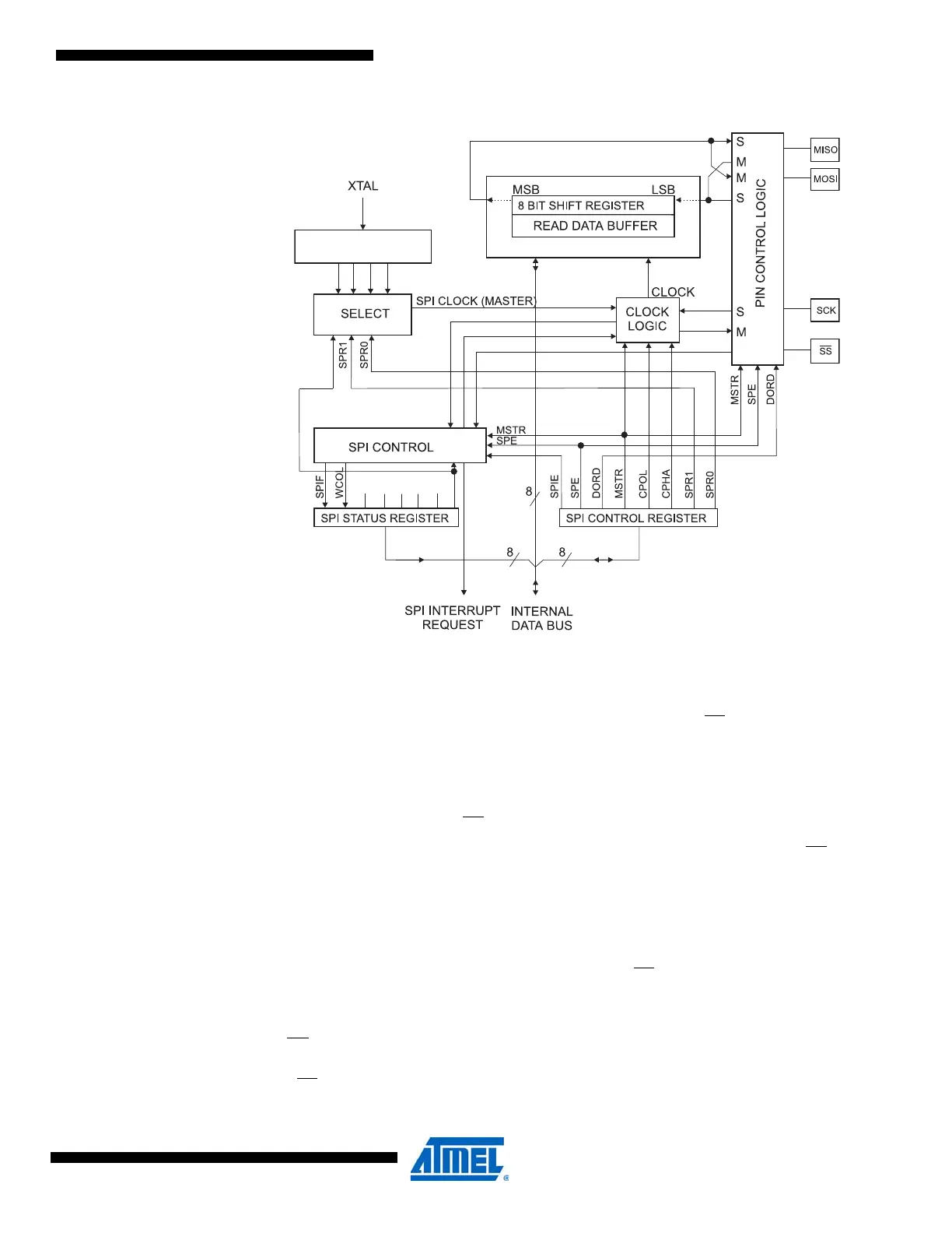
Figure 19-1. SPI Block Diagram
(1)
Note: 1. Refer to Figure 1-1 on page 2, and Table 14-3 on page 84 for SPI pin placement.
The interconnection between Master and Slave CPUs with SPI is shown in Figure 19-2 on page
170. The system consists of two shift Registers, and a Master clock generator. The SPI Master
initiates the communication cycle when pulling low the Slave Select SS
pin of the desired Slave.
Master and Slave prepare the data to be sent in their respective shift Registers, and the Master
generates the required clock pulses on the SCK line to interchange data. Data is always shifted
from Master to Slave on the Master Out – Slave In, MOSI, line, and from Slave to Master on the
Master In – Slave Out, MISO, line. After each data packet, the Master will synchronize the Slave
by pulling high the Slave Select, SS
, line.
When configured as a Master, the SPI interface has no automatic control of the SS
line. This
must be handled by user software before communication can start. When this is done, writing a
byte to the SPI Data Register starts the SPI clock generator, and the hardware shifts the eight
bits into the Slave. After shifting one byte, the SPI clock generator stops, setting the end of
Transmission Flag (SPIF). If the SPI Interrupt Enable bit (SPIE) in the SPCR Register is set, an
interrupt is requested. The Master may continue to shift the next byte by writing it into SPDR, or
signal the end of packet by pulling high the Slave Select, SS
line. The last incoming byte will be
kept in the Buffer Register for later use.
When configured as a Slave, the SPI interface will remain sleeping with MISO tri-stated as long
as the SS
pin is driven high. In this state, software may update the contents of the SPI Data
Register, SPDR, but the data will not be shifted out by incoming clock pulses on the SCK pin
until the SS
pin is driven low. As one byte has been completely shifted, the end of Transmission
Flag, SPIF is set. If the SPI Interrupt Enable bit, SPIE, in the SPCR Register is set, an interrupt
SPI2X
SPI2X
DIVIDER
/2/4/8/16/32/64/128