ATtiny10/11/12
14
I/O Memory
The I/O space definition of the ATtiny10/11/12 is shown in the following table:
Note: Reserved and unused locations are not shown in the table.
All the different ATtiny10/11/12 I/O and peripherals are placed in the I/O space. The different I/O locations are accessed by
the IN and OUT instructions transferring data between the 32 general-purpose working registers and the I/O space. I/O reg-
isters within the address range $00 - $1F are directly bit-accessible using the SBI and CBI instructions. In these registers,
the value of single bits can be checked by using the SBIS and SBIC instructions. Refer to the Instruction Set Summary for
more details.
For compatibility with future devices, reserved bits should be written to zero if accessed. Reserved I/O memory addressed
should never be written.
The different I/O and peripherals control registers are explained in the following sections.
Status Register – SREG
The AVR status register (SREG) at I/O space location $3F is defined as:
•
Bit 7 - I: Global Interrupt Enable
The global interrupt enable bit must be set (one) for the interrupts to be enabled. The individual interrupt enable control is
then performed in separate control registers. If the global interrupt enable register is cleared (zero), none of the interrupts
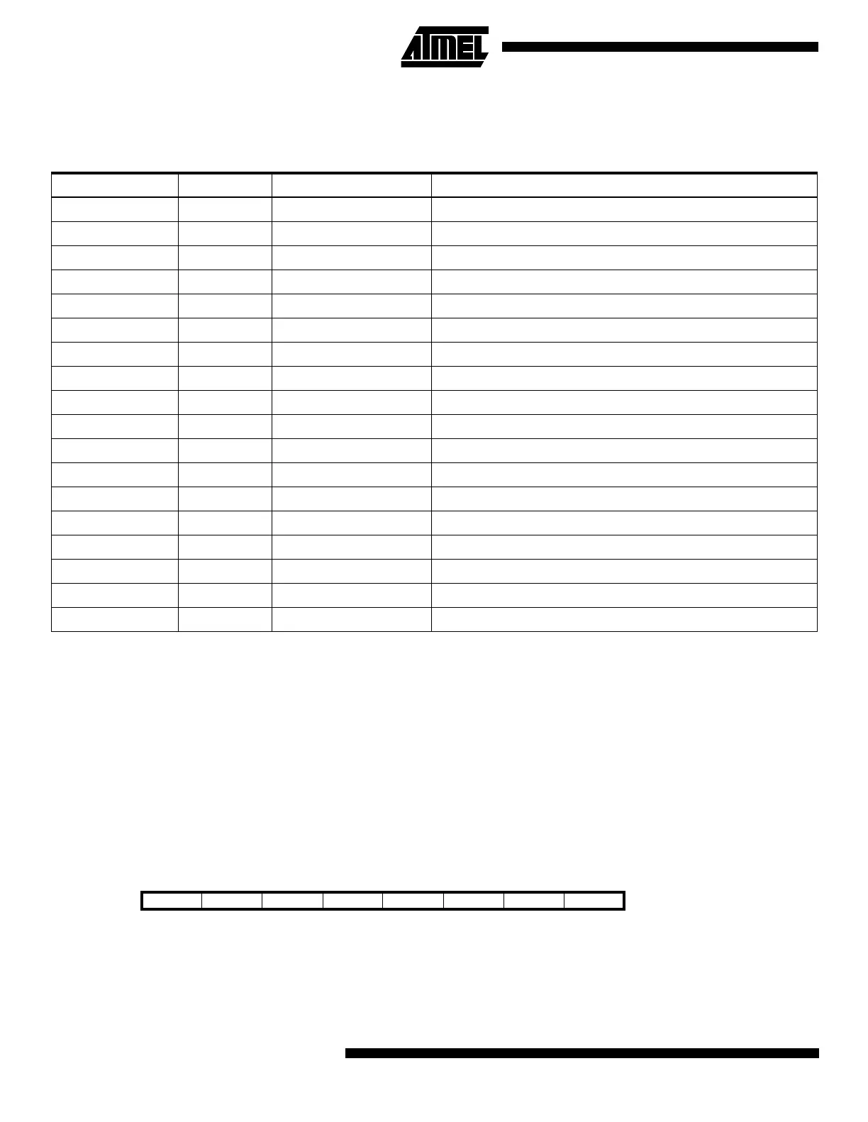
Table 4. ATtiny10/11/12 I/O Space
Address Hex Name Device Function
$3F SREG ATtiny10/11/12 Status Register
$3B GIMSK ATtiny10/11/12 General Interrupt Mask Register
$3A GIFR ATtiny10/11/12 General Interrupt Flag Register
$39 TIMSK ATtiny10/11/12 Timer/Counter Interrupt Mask Register
$38 TIFR ATtiny10/11/12 Timer/Counter Interrupt Flag Register
$35 MCUCR ATtiny10/11/12 MCU Control Register
$34 MCUSR ATtiny10/11/12 MCU Status Register
$33 TCCR0 ATtiny10/11/12 Timer/Counter0 Control Register
$32 TCNT0 ATtiny10/11/12 Timer/Counter0 (8-bit)
$31 OSCCAL ATtiny12 Oscillator Calibration Register
$21 WDTCR ATtiny10/11/12 Watchdog Timer Control Register
$1E EEAR ATtiny12 EEPROM Address Register
$1D EEDR ATtiny12 EEPROM Data Register
$1C EECR ATtiny12 EEPROM Control Register
$18 PORTB ATtiny10/11/12 Data Register, Port B
$17 DDRB ATtiny10/11/12 Data Direction Register, Port B
$16 PINB ATtiny10/11/12 Input Pins, Port B
$08 ACSR ATtiny10/11/12 Analog Comparator Control and Status Register
Bit 76543210
$3F I T H S V N Z C SREG
Read/Write R/W R/W R/W R/W R/W R/W R/W R/W
Initial value 0 0 0 0 0 0 0 0
 Loading...


