42
ATtiny15L
1187H–AVR–09/07
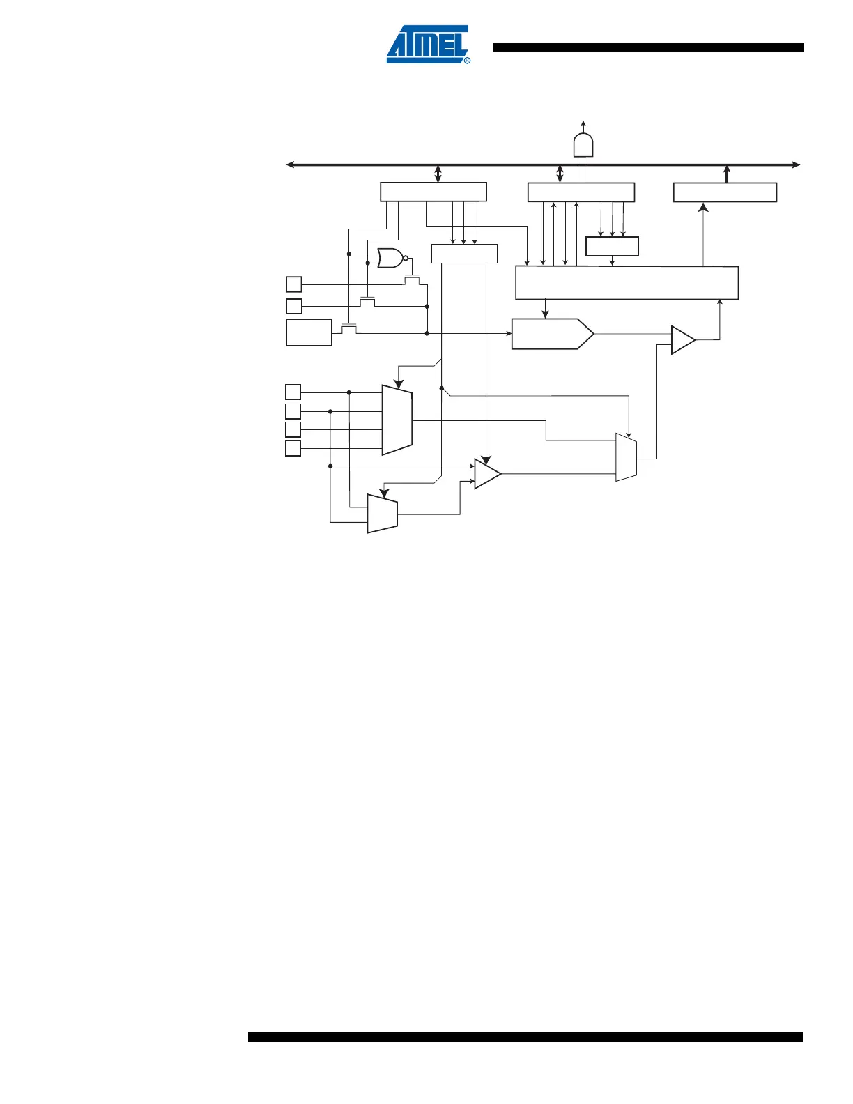
Figure 25. Analog-to-Digital Converter Block Schematic
Operation The ADC converts an analog input voltage to a 10-bit digital value through successive
approximation. The minimum value represents GND and the maximum value represents
the selected reference voltage minus 1 LSB.
The voltage reference for the ADC may be selected by writing to the REFS1..0 bits in
ADMUX. V
CC
, the AREF pin, or an internal 2.56V reference may be selected as the ADC
voltage reference. Optionally, the 2.56V internal voltage reference may be decoupled by
an external capacitor at the AREF pin to improve noise immunity.
The analog input channel and differential gain are selected by writing to the MUX2..0
bits in ADMUX. Any of the four ADC input pins ADC3..0 can be selected as single-
ended inputs to the ADC. ADC2 and ADC3 can be selected as positive and negative
input, respectively, to the differential gain amplifier.
If differential channels are selected, the differential gain stage amplifies the voltage dif-
ference between the selected input pair by the selected gain factor, 1x or 20x, according
to the setting of the MUX2..0 bits in ADMUX. This amplified value then becomes the
analog input to the ADC. If single-ended channels are used, the gain amplifier is
bypassed altogether.
If ADC2 is selected as both the positive and negative input to the differential gain ampli-
fier (ADC2 - ADC2), the remaining offset in the gain stage and conversion circuitry can
be measured directly as the result of the conversion. This figure can be subtracted from
subsequent conversions with the same gain setting to reduce offset error to below 1
LSB.
The ADC can operate in two modes – Single Conversion and Free Running. In Single
Conversion mode, each conversion will have to be initiated by the user. In Free Running
ADC CONVERSION
COMPLETE IRQ
8-BIT DATA BUS
90
ADC MULTIPLEXER
SELECT (ADMUX)
ADC CTRL. & STATUS
REGISTER (ADCSR)
ADC DATA REGISTER
(ADCH/ADCL)
MUX2
ADIE
ADFR
ADSC
ADEN
ADIF
ADIF
MUX1
MUX0
ADPS0
ADPS1
ADPS2
CONVERSION LOGIC
10-BIT DAC
+
-
SAMPLE & HOLD
COMPARATOR
INTERNAL
2.56 V
REFERENCE
MUX DECODER
VCC
AREF
ADC3
ADC2
ADC1
ADC0
REFS0
REFS1
ADLAR
+
-
CHANNEL SELECTION
GAIN SELECTION
ADC[9:0]
GAIN
AMPLIFIER
PRESCALER
SINGLE ENDED / DIFFERENTIAL SELECTION
POS.
INPUT
MUX
NEG.
INPUT
MUX

 Loading...


