46
ATtiny15L
1187H–AVR–09/07
ADC Noise Canceler
Function
The ADC features a noise canceler that enables conversion during ADC Noise Reduc-
tion mode (see “Sleep Modes” on page 23) to reduce noise induced from the CPU core
and other I/O peripherals. If other I/O peripherals must be active during conversion, this
mode works equivalently for Idle mode. To make use of this feature, the following proce-
dure should be used:
1. Make sure that the ADC is enabled and is not busy converting. Single Conver-
sion mode must be selected and the ADC conversion complete interrupt must be
enabled.
ADEN = 1
ADSC = 0
ADFR = 0
ADIE = 1
2. Enter ADC Noise Reduction mode (or Idle mode). The ADC will start a conver-
sion once the CPU has been halted.
3. If no other interrupts occur before the ADC conversion completes, the ADC inter-
rupt will wake up the MCU and execute the ADC conversion complete interrupt
routine.
The ADC Multiplexer Selection
Register – ADMUX
• Bits 7..6 – REFS1..REFS0: Reference Selection Bits
These bits select the voltage reference for the ADC, as shown in Table 19. If these bits
are changed during a conversion, the change will not go into effect until this conversion
is complete (ADIF in ADCSR is set). Whenever these bits are changed, the next
conversion will take 25 ADC clock cycles. If active channels are used, using AVCC or an
external AREF higher than (AVCC - 1V) is not recommended, as this will affect ADC
accuracy. The internal voltage reference options may not be used if an external
reference voltage is being applied to the AREF pin.
• Bit 5 – ADLAR: ADC Left Adjust Result
The ADLAR bit affects the presentation of the ADC conversion result in the ADC Data
Register. If ADLAR is cleared, the result is right-adjusted. If ADLAR is set, the result is
left-adjusted. Changing the ADLAR bit will affect the ADC Data Register immediately,
regardless of any ongoing conversions. For a complete description of this bit, see “The
ADC Data Register – ADCL and ADCH” on page 49.
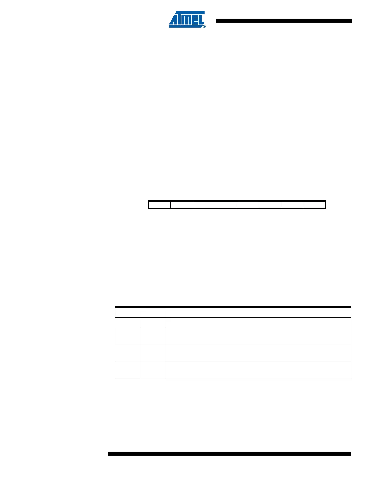
Bit 76543210
$07 REFS1 REFS0 ADLAR – – MUX2 MUX1 MUX0 ADMUX
Read/Write R/W R/W R/W R R R/W R/W R/W
Initial Value00000000
Table 19. Voltage Reference Selections for ADC
REFS1 REFS0 Voltage Reference Selection
00V
CC
used as analog reference, disconnected from PB0 (AREF).
01
External Voltage Reference at PB0 (AREF) pin, Internal Voltage
Reference turned off.
10
Internal Voltage Reference without external bypass capacitor,
disconnected from PB0 (AREF).
11
Internal Voltage Reference with external bypass capacitor at PB0 (AREF)
pin.

 Loading...


