56
ATtiny15L
1187H–AVR–09/07
High-voltage Serial
Programming Algorithm
To program and verify the ATtiny15L in the High-voltage Serial Programming mode, the
following sequence is recommended (See instruction formats in Table 25):
1. Power-up sequence:
Apply 4.5 - 5.5V between V
CC
and GND. Set PB5 and PB0 to “0” and wait at least
30 µs.
Set PB3 to “0”. Wait at least 100 ns.
Apply 12V to PB5 and wait at least 100 ns before changing PB0. Wait 8 µs
before giving any instructions.
2. The Flash array is programmed one byte at a time by supplying first the address,
then the low and high data byte. The write instruction is self-timed; wait until the
PB2 (RDY/BSY
) pin goes high.
3. The EEPROM array is programmed one byte at a time by supplying first the
address, then the data byte. The write instruction is self-timed; wait until the PB2
(RDY/BSY
) pin goes high.
4. Any memory location can be verified by using the Read instruction, which
returns the contents at the selected address at serial output PB2.
5. Power-off sequence:
Set PB3 to “0”.
Set PB5 to “0”.
Turn V
CC
power off.
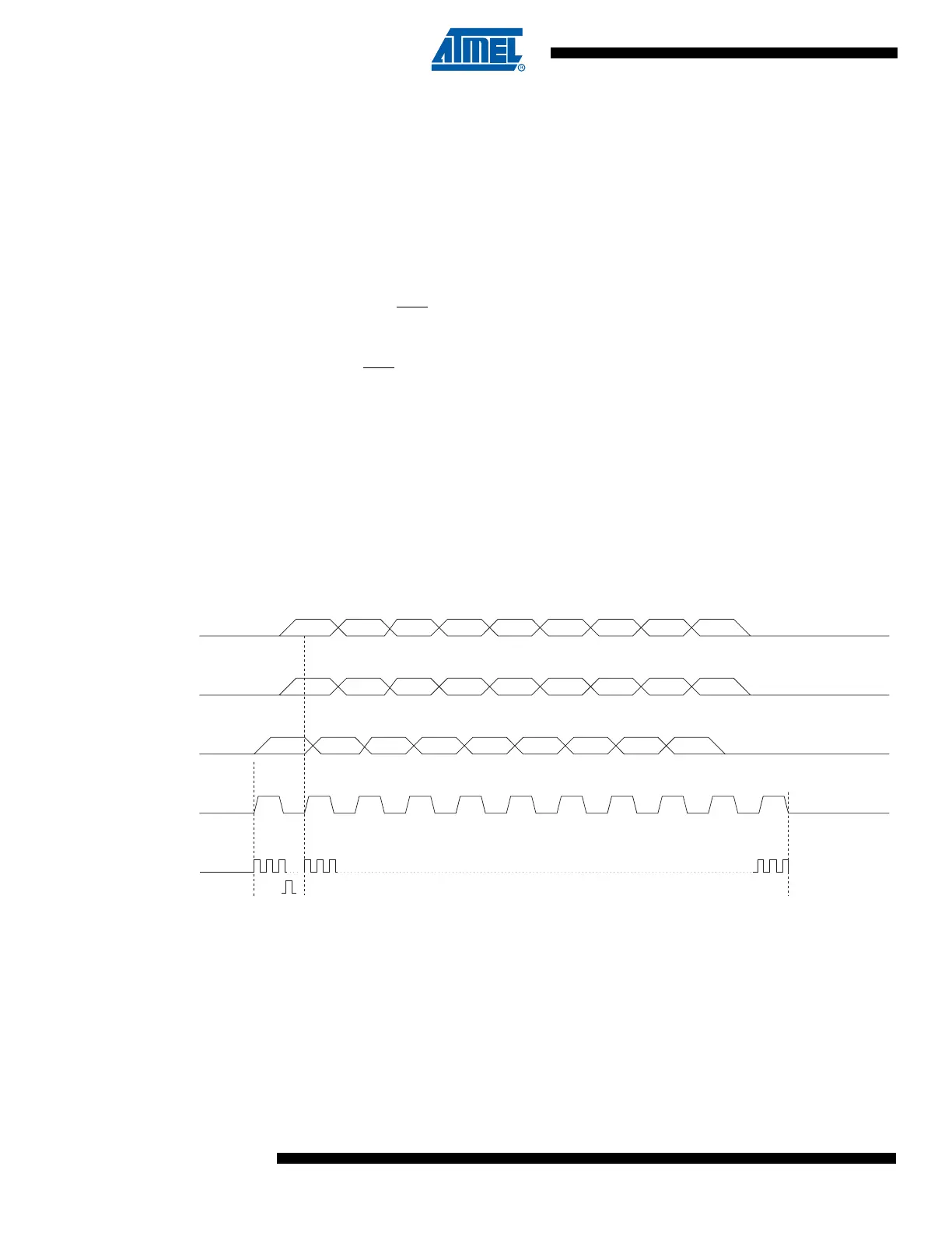
When writing or reading serial data to the ATtiny15L, data is clocked on the eigth rising
edge of the 16 external clock pulses needed to generate the internal clock. See Figure
31, Figure 32, and Table 26 for an explanation.
Figure 31. High-voltage Serial Programming Waveforms
MSB
MSB
MSB LSB
LSB
LSB
012345678910
SERIAL DATA INPUT
PB0
SERIAL INSTR. INPUT
PB1
SERIAL DATA OUTPUT
PB2
INTERNAL CK
SERIAL CLOCK INPUT
PB3
16x

 Loading...


