Do you have a question about the Avnet MicroZed and is the answer not in the manual?
Details the Zynq bank pin assignments for the MicroZed, showing I/O connections.
Details the optional 1Kb SHA Security EEPROM footprint and its functionality.
Describes the 100 MHz single-ended clock source connected to the Zynq AP SOC.
Explains the different reset sources available on the carrier card, including buttons.
Covers user accessible I/O components like push buttons, LEDs, and DIP switches.
Information on the interface connectors for expansion and system integration.
Covers the XADC header for analog reference designs and AMS daughter cards.
Details the JTAG connector for programming and debugging the MicroZed.
Information on power input, voltage regulators, sequencing, and power good indicator.
Provides a quick reference for jumpers, configuration settings, and test points on the IOCC.
Provides horizontal mechanical dimensions of the IOCC in mils and visual representations of height.
Specifies the weight of the IOCC with populated jumpers and rubber feet.
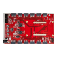
The MicroZed I/O Carrier Card (IOCC) is an evaluation board designed to expand the input/output capabilities of MicroZed System On Module (SOM) boards, specifically the Avnet MicroZed 7Z010 or 7Z020 products. Its primary function is to provide accessible SoC I/O pins from the MicroZed SOM board through 12 Pmod connectors. Beyond I/O access, the IOCC also supplies power to the SOM board via JX MicroHeaders.
The board integrates a variety of user interface features, including eight user LEDs, four user push buttons, and four DIP switches, allowing for flexible interaction and configuration. For programming and debugging, the IOCC provides a Xilinx PC4 Header that accesses the PL JTAG.
For memory, the IOCC features an optional footprint for a 1KB 1-wire SHA Security EEPROM, though this component is not populated by default. This EEPROM, if installed, would offer secure authentication and data storage capabilities.
The IOCC incorporates a 100MHz single-ended on-board oscillator, controlled by the FPGA, which connects to one of the MRCC pins in PL bank 35, enabling direct connection to internal MMCMs and PLLs of the Zynq AP SoC. The FPGA activates this clock via the BB_CLK_EN signal, which is pulled low by default, keeping the clock off until enabled.
Power management is a key aspect of the IOCC. It supports a primary 5V input (≥ 2.0 A) and includes internal power regulation. This includes filtered 5V for the XADC, high-efficiency regulators (85%+) for 1.8V/2.5V/3.3V at 2.3A (for Module VCCIO Bank 34) and 2.85A (for Module VCCIO Bank 35 and Bank 13, if a 7Z020 MicroZed is used). Additionally, a low-noise LDO provides a 1.8V at 0.15A supply for the XADC, and a 0.2% accurate 1.25V at 0.05A precision reference for the XADC. The board's input voltage is supplied through a 2.5mm/5.5mm inner/outer, center-positive barrel jack, CON2, with an input voltage range of 5V to 12V. The default power supply provided by Avnet is a 5V, 2 Ampere supply suitable for general low-power I/O applications and XADC header use.
The IOCC also features several reset sources. The INIT# button (SW3) provides an active-low input signal to the FPGA, used to stall the power-on configuration sequence. The POR# button (SW2) provides an active-low signal to the PG_CARRIER net, resetting the USB UART, USB OTG circuit, and turning off the IOCC VCCIO_34/35 power supplies, initiating a total system power reset for both the IOCC and MicroZed. The SYS_RST# button (SW4) provides an active-low signal to CARRIER_SRST#, resetting functional logic within the device without disturbing the debug environment, and also resets the PL.
The Pmod compatible expansion headers (2x6) are a central feature, with 12 right-angle 0.1" female headers. These connections provide eight user I/O lines and an adjustable voltage derived from VCCIO_34 and VCCIO_35 power supplies, selectable to 1.8V, 2.5V, or 3.3V. When 3.3V is selected, the connectors are Pmod compatible. Most Pmod connections are matched differential and routed differentially to ensure high-speed signal integrity. The PS Pmod, connected to bank 500, can be used for PJTAG access (MIO[10-13]) and other hardened MIO peripherals. For 7Z020 MicroZed devices, Pmods JY and JZ are sourced by Bank 13.
Two MicroHeaders (TE PN: 5177984-4) connect the IOCC to the MicroZed, providing access to Zynq PL I/O, eight PS-GPIO, six dedicated analog inputs, and four dedicated JTAG signals. These connectors are FCI BERGSTAK 0.8mm pitch, with variable stack heights from 5mm to 20mm, facilitating connection to various expansion boards. Each 100-pin connector carries I/O, analog signals, power, and ground. The Carrier powers the MicroZed, offering an alternative to USB-UART power. Each pin can carry 500mA of current and is certified for PCIe Gen2 bandwidth. The Carrier is responsible for powering the PL VCCIO banks, allowing flexible control over I/O bank voltages. The 7Z010 has two PL I/O banks (34 and 35), each with 50 I/O, while the 7Z020 adds a third I/O bank (13). Within a PL I/O bank, there are 50 I/O capable of 24 differential pairs, supporting DDR data at up to 950Mbps for -1 speed grade devices. Eight I/O can be used as clock inputs. Bank 35 supports up to 16 differential analog inputs.
The Agile Mixed Signaling (AMS) interface, provided by the XADC header, offers analog connectivity for reference designs, including AMS daughter cards. The pinout is designed for tightly coupled differential analog pairs and AGND isolation between channels. Anti-aliasing filters are used for the XADC inputs (VP/VN, VAUX0P/VAUX0N, VAUX8P/VAUX8N). If the XADC function is not needed, the port can be repurposed for additional GPIO expansion, with VCCIO_35 setting the acceptable voltage levels for XADC_GIOx signals.
For maintenance, the IOCC includes a green status LED that indicates when PG_CARRIER and/or PG_MODULE is "good," signifying proper power supply operation. The board also features various jumpers, configuration settings, and test points for easy setup and troubleshooting. For instance, jumpers control PUDC# (active low), JTAG (Zynq JTAG interface), and VBAT (+1.8V for FPGA battery support). DIP switches (DIP_SW0-3) provide four user-selectable switches to the Zynq PL fabric, pulled low in the OFF position and connected to VCCIO_35 in the ON position. Test points are available for monitoring signals like CARRIER_SRST, GND, A1V8, VREF_1V25, VCCIO_34, VCCIO_35, and 3V3. Connectors CON3 and CON4 allow for selecting +3.3V settings for VCCIO_34 and VCCIO_35, respectively. The board's design adheres to recommended decoupling techniques per manufacturer datasheets to ensure stable power delivery.
| Storage | MicroSD card slot |
|---|---|
| Clocking | 33.333 MHz oscillator |
| Processor | Xilinx Zynq-7000 SoC |
| FPGA | Xilinx Zynq-7000 |
| Memory | 512 MB DDR3 |
| Ethernet | 10/100/1000 Mbps Ethernet |
| USB | USB 2.0 (OTG) |
| Expansion | FMC |
| Power | 5V |
| Operating Temperature | 0°C to +70°C (Commercial), -40°C to +85°C (Industrial) |