13
CONFIGURATION PROCEDURE
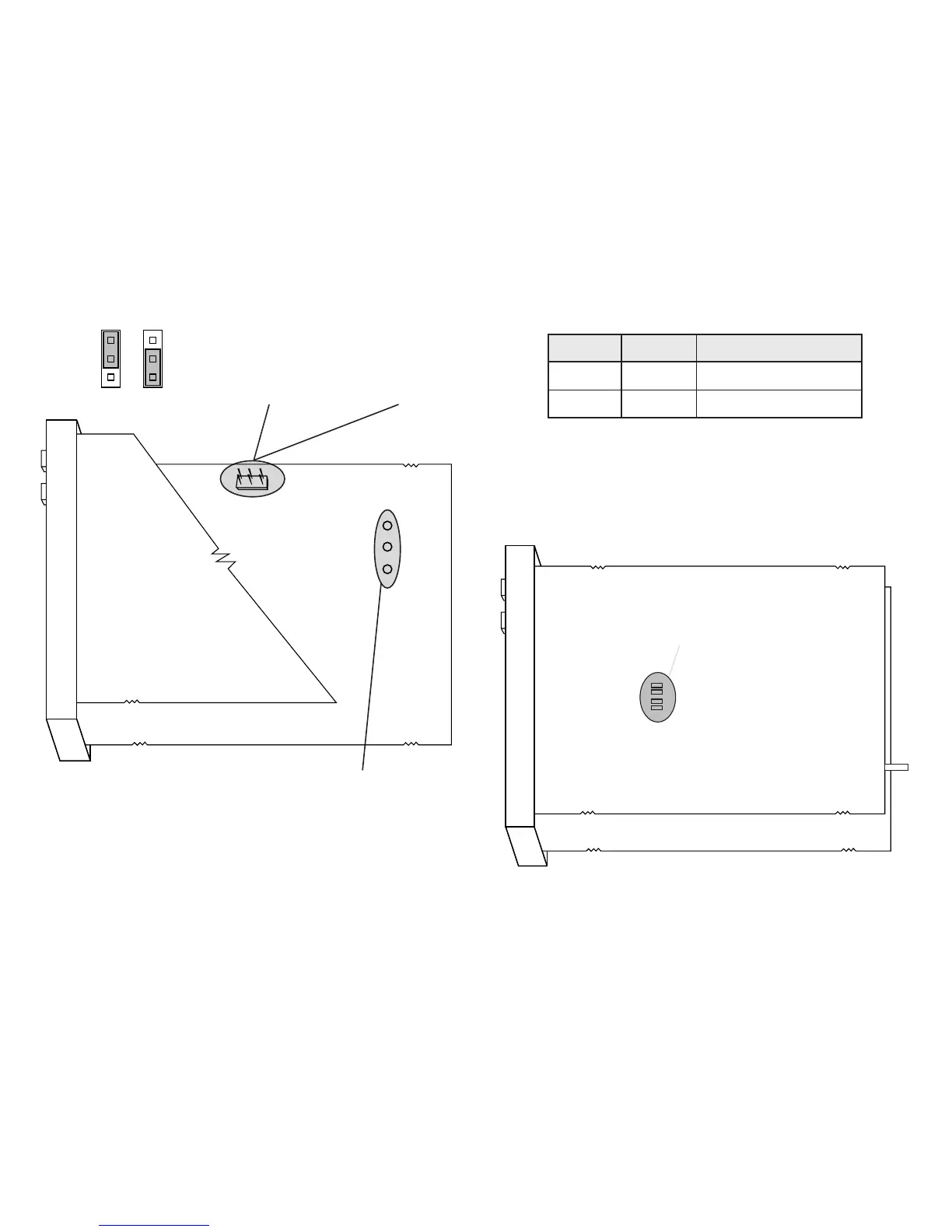
Preliminary Hardware Settings
1) Remove the instrument from its case.
2) Set J303, J304 and J305 as shown below:
J303
(AL1, Cool)
1 - 2 = Out NO (default)
2 - 3 = Out NC
J305
(MAIN output)
1 - 2 = SSR
2 - 3 = Relay
J304
(AL1, Cool)
1 - 2 = SSR
2 - 3 = Relay
1
3
NOTE: J303 is a solder jumper and is on
the component side of the PCB.
Figure 1
Open input circuit
This instrument is able to identify an open circuit for TC
and RTD inputs. The open input circuit condition for RTD
input is shown by an “overrange” indication. For TC
input, either an overrange indication (standard) or
underrange indication can be selected from the following
table:
2HS 2HC noitacidnI
nepoesolc)tluafed(egnarrevo
esolcnepoegnarrednu
Both pads are located on the solder side of the CPU card.
CAUTION: Solder carefully to avoid damage to PCB or
other components.
SH2
CH2
 Loading...