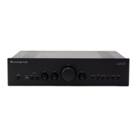
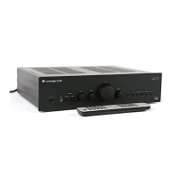
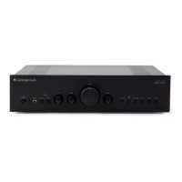
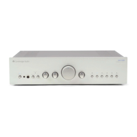
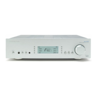
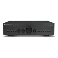
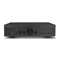
540A V2.0 SERVICE MANUAL
TABLE OF CONTENTS
Safety Precautions & Important Notes
3
Exploded Diagram 4
Input PCB Schematic (Power Supply) 5
Input PCB Schematic (Buffers and Switches) 6
Input PCB Schematic (Tone Control) 7
Input PCB Schematic (Protection Circuitry) 8
Input PCB Schematic (Headphone Driver) 9
Input PCB Layout (Top Side) 10
Input PCB Layout (Bottom Side) 11
Input PCB Assembly BOM 12-13
Voltage Select Switch PCB Schematic 14
Voltage Select PCB Layout (Top Side) 15
Voltage Select PCB Layout (Bottom Side) 16
Voltage Select PCB Assembly BOM 17
Mains PCB Schematic 18
Front Panel PCB Schematic 19
Mains & Front Panel PCB Layout (Top Side) 20
Mains & Front Panel PCB Layout (Bottom Side) 21
Mains & Front Panel PCB Assembly BOM 22
Amp PCB Schematic (Right Channel) 23
Amp PCB Schematic (Protection) 24
Amp PCB Schematic (Power Amp) 25
Amp PCB Schematic (Left Channel) 26
Amp PCB Layout (Top Side) 27
Amp PCB Layout (Bottom Side) 28
Amp PCB Assembly BOM 29-31
Abus Module PCB Schematic 32
Abus Module PCB Layout (Top Side) 33
Abus Module PCB Layout (Bottom Side) 34
Abus PCB Assembly BOM 35
IC Pin Layout Details 36-42