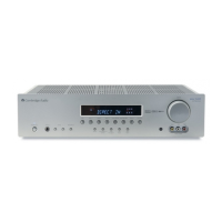
Do you have a question about the Cambridge Audio 540R V2.0 and is the answer not in the manual?
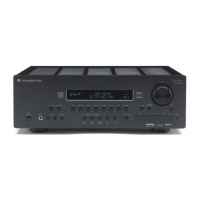
Comprehensive list of all components used in the AV receiver.
Pin configurations for various integrated circuits.
Circuit diagrams for the decoder PCB.
Physical layout of components on the decoder PCB.
Circuit diagrams for the main board's power supply, output, and protection.
Physical layout of components on the main board.
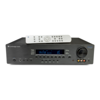
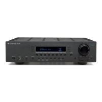
| Channels | 6.1 |
|---|---|
| Frequency Response | 10 Hz - 50 kHz |
| Input Impedance | 47 kOhm |
| Input Sensitivity | 200 mV |
| Tuner Bands | FM/AM |
| Audio D/A Converter | 24-bit/192 kHz |
| Width | 430 mm |
| Depth | 350 mm |
| Amplifier Type | Class AB |
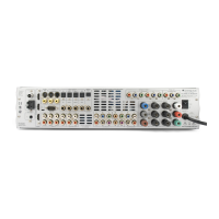
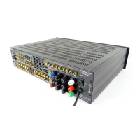
| Inputs | 2 x Optical, 1 x Coaxial |
| Outputs | 1 x Subwoofer |