Do you have a question about the Cambridge Audio 651A and is the answer not in the manual?
Detailed safety instructions for proper and safe operation of the unit.
Information on regulatory compliance, symbols, and warnings.
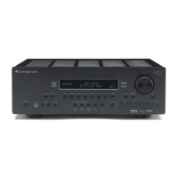
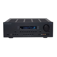
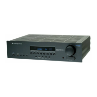
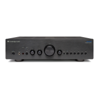
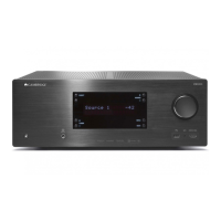
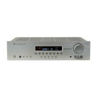
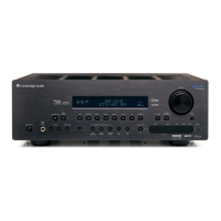
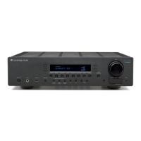
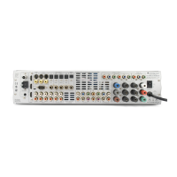
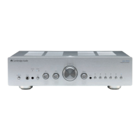
Visual representation of the unit's components for identification.
List of replacement parts with part numbers and descriptions.
Circuit diagram for the front panel control board.
Physical layout of components and traces on the front panel PCB.
Bill of Materials for the front panel control PCB.
Circuit diagram for the input signal processing board.
Physical layout of components and traces on the input PCB.
Bill of Materials for the input signal processing PCB.
Circuit diagram for the pre-amplifier and control circuitry.
Continuation of the pre-amplifier and control circuitry schematic.
Physical layout of components and traces on the pre-amplifier PCB.
Bill of Materials for the pre-amplifier and control PCB.
Circuit diagram for the unit's protection circuitry.
Physical layout of components and traces on the protection PCB.
Bill of Materials for the protection circuitry PCB.
Circuit diagram for the speaker output stage and protection.
Physical layout of components and traces on the speaker output PCB.
Bill of Materials for the speaker output PCB.
Circuit diagram for the left channel power amplifier stage.
Circuit diagram for the right channel power amplifier stage.
Continuation of the power amplifier stage schematic.
Physical layout of components and traces on the power amplifier PCB.
Bill of Materials for the power amplifier stage PCB.
Instructions for routing and securing internal wires during assembly.
Details on transistor mounting hardware and bracket screws.
Circuit diagram and BOM for the EU mains input and power filtering.
Circuit diagram and BOM for the CU (115V) mains input and power filtering.
Circuit diagram for the USB audio interface board.
Physical layout of components and traces on the USB audio PCB.
Bill of Materials for the USB audio interface PCB.
Pin configuration for ICs used on the Input PCB.
Pin configuration for ICs used on the Preamp PCB.
Pin configuration for ICs used on the Power Amp PCB.
Pin configuration for ICs used on the Mains PCB.
Pin configuration for ICs used on the Speaker PCB.
Pin configuration for ICs used on Volume and Protection PCBs.
Details on part revisions and modifications for Auto Power Down (APD) functionality.
Schematic of the Input PCB showing APD integration.
Schematic of the Preamp PCB showing APD integration.
Circuit diagram for the APD trigger signal generation board.
Specification for the cable connecting APD components.
Description of the headphone output driver and mute functionality.
Circuit diagram for the voltage and current protection system.
| S/N Ratio | >92dB (unweighted) |
|---|---|
| Input Impedance | 47k ohms |
| Power Consumption | 600W |
| Damping Factor | >100 |
| Power Output | 75W RMS into 8 Ohms |
| THD (unweighted, 20Hz-20kHz) | <0.02% |
| Frequency Response | 5Hz - 50kHz (+/-1dB) |
| Inputs | 1 x 3.5mm (Front Aux) |