5
5
4
4
3
3
2
2
1
1
D D
C C
B B
A A
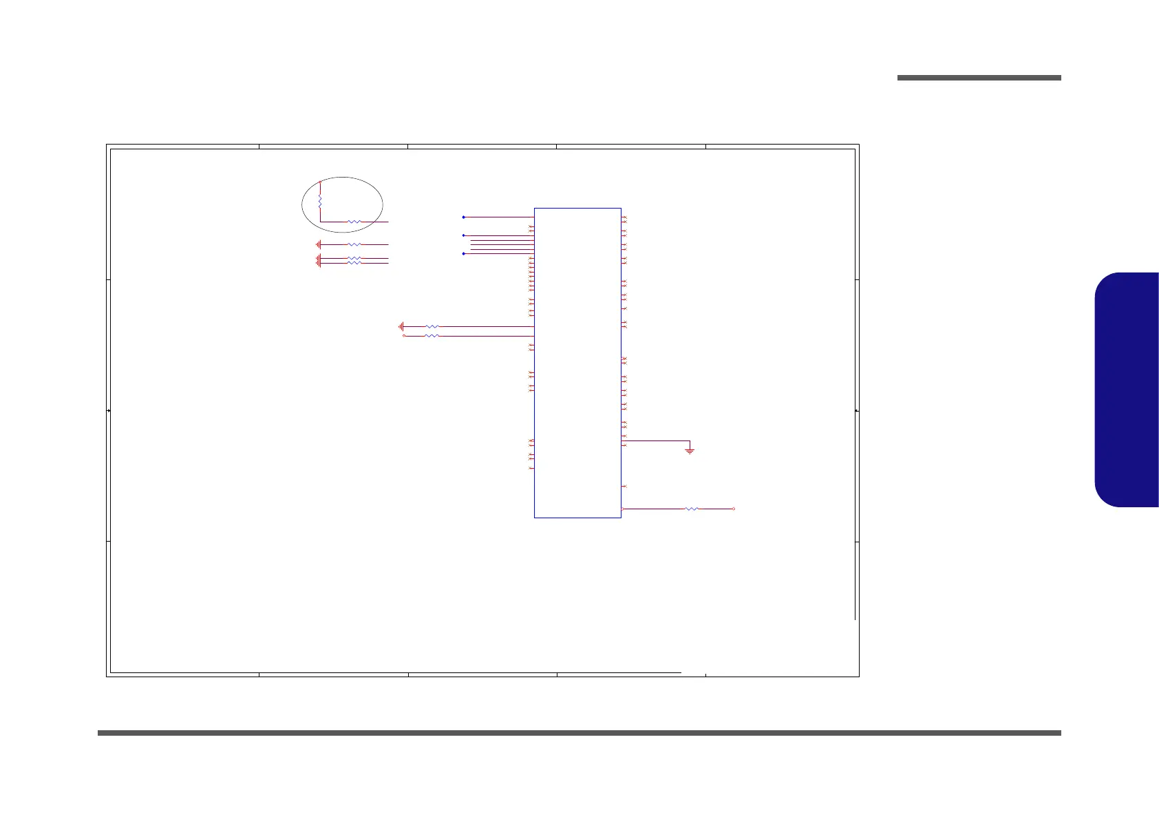
CFG[0]: Stall reset sequence after PCU PLL
Ʉ
lock until de-asserted:
— 1 = (Default) Normal Operation; No
stall.
— 0 = Stall.
CFG[1]: Reserved configuration lane.
Ʉ
CFG[2]: PCI Express* Static x16 Lane
Ʉ
Numbering Reversal.
— 1 = Normal operation
— 0 = Lane numbers reversed.
CFG[3]: Reserved configuration lane.
Ʉ
CFG[4]: eDP enable:
Ʉ
— 1 = Disabled.
— 0 = Enabled.
CFG[6:5]: PCI Express* Bifurcation
Ʉ
— 00 = 1 x8, 2 x4 PCI Express*
— 01 = reserved
— 10 = 2 x8 PCI Express*
— 11 = 1 x16 PCI Express*
CFG[7]: PEG Training:
Ʉ
— 1 = (default) PEG Train immediately
following RESET# de assertion.
— 0 = PEG Wait for BIOS for training.
CFG[19:8]: Reserved configuration lanes.
Ʉ
check ok
2018/6/27
1.05VA
3.3VA
VCCIO
Title
Size Document Number Rev
Date: Sheet
of
6-71-N15Z0-D01
D01
[04] WHL U D,Q/20 CFG
A3
446Wednesday, August 29, 2018
ᙔ!Ϻ!ႝ!တ!!DMFWP!DP/
N150ZU
Title
Size Document Number Rev
Date: Sheet
of
6-71-N15Z0-D01
D01
[04] WHL U D,Q/20 CFG
A3
446Wednesday, August 29, 2018
ᙔ!Ϻ!ႝ!တ!!DMFWP!DP/
N150ZU
Title
Size Document Number Rev
Date: Sheet
of
6-71-N15Z0-D01
D01
[04] WHL U D,Q/20 CFG
A3
446Wednesday, August 29, 2018
ᙔ!Ϻ!ႝ!တ!!DMFWP!DP/
N150ZU
R71
*150_04
R436*1K_04
R4321K_04
R442 1.5K_04
R72*1K_04
R427 10K_04
20 of 20
WHL QS/CFL/WHL_ES1_CNL U
U25Q
WHL_U_IP_CCG/BGA
ITP_PMODE
W4
RSVD_TP_12
CN36
CFG_18
N3
RSVD_TP_13/RSVD/RSVD_TP_13
AT3
CFG_19
N4
RSVD_10
H4
TP_1
BP35
RSVD_11
H3
TP_2
BP34
IST_TP_0/RSVD/IST_TP_0
AL2
RSVD_12
BV24
TP_3
BK34
IST_TP_1/RSVD/IST_TP_1
AL1
RSVD_TP_1/RSVD/RSVD_TP_1
AU3
CFG_0
T4
RSVD_13
BV25
TP_4
BR18
RSVD_TP_2/RSVD/RSVD_TP_2
CR35
CFG_1
R4
RSVD_14
CR4
RSVD_TP_3/RSVD/RSVD_TP_3
BJ36
SKTOCC#
E1
CFG_2
T3
RSVD_15
CP3
VSS_1/TP/VSS_1
BP36
RSVD_TP_4/RSVD/RSVD_TP_4
BJ34
RSVD_2
AN1
CFG_3
R3
RSVD_16
CR3
CFG_RCOMP
AB5
RSVD_TP_5
F37
RSVD_3
AN2
RSVD_17
BK35
CFG_4
J4
RSVD_4
W3
IST_TRIG_0/RSVD/IST_TRIG_0
AL4
RSVD_TP_6
F34
RSVD_18
BK36
CFG_10
R1
CFG_5
M4
RSVD_5
AM4
IST_TRIG_1/RSVD/IST_TRIG_1
AL3
RSVD_TP_7/RSVD/RSVD_TP_7
AM3
CFG_11
N1
CFG_6
J3
RSVD_TP_8/RSVD/RSVD_TP_8
BT9
RSVD_6
AN4
CFG_12
J2
CFG_7
M3
RSVD_TP_9/RSVD/RSVD_TP_9
BT8
RSVD_7
AN3
CFG_13
L2
CFG_8
R2
RSVD_8
CG2
CFG_14
J1
CFG_9
N2
RSVD_9
CG1
CFG_15
L1
IST_TRIG
CP36
CFG_16
L3
RSVD_TP_10/RSVD/RSVD_TP_10
BP8
CFG_17
L4
RSVD_TP_11/RSVD/RSVD_TP_11
BP9
R74 49.9_1%_04
R431*1K_04
CFG5
CFG6
CFG7
CFG4
CFG3
CFG_RCOMP
SKTOCC#
CFG0
CFG4
CFG6
CFG5
CFG0