CMT2310A
Rev 1.0E | Page44/50
8 User Register
All configuration and control operations from external MCU are accomplished by accessing the registers in the 3 pages through
SPI interface. Shifting among the 3 pages will be accomplished through writing the address 0x7E. As shown in the table below,
the address range 0x00 ~ 0x71 are divided into 3 banks for understanding purpose, configuration bank (including 6 sub-banks),
control bank 1 and control bank 2, which will be detailed below.
The addresses of the 3 banks are continuous. Operation method against the 3 banks have no essential difference, namely all
operations are direct read/write operations following the SPI register read/write timing. However, for the 3 banks the
functionalities and usage are different as shown in the table below.
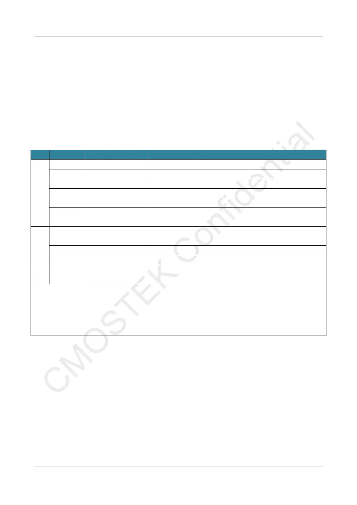
Table 21. CMT2310A Register Bank Partitioning
For chip operation and control like state switching, status checking, etc.
For chip function enabling.
For reading and clearing interrupt flag, unaccessible in SLEEP state.
Configuration bank
(packet format)
For packet format and FIFO related configurations.
Configuration bank
(system feature)
For system operating related function configurations.
Configuration bank (CMT
internal use)
For CMT internal use only.
For transmitter related feature configurations.
For receiver related feature configurations.
Configuration bank (auto-
frequency hopping)
For storing automatic channel hopping table information.
Notes:
1. In Page 0, address 0x7A is FIFO accessing interface address, address 0x7B is the interface for continuously accessing
register.
2. In all Pages, address 0x7E is the interface for Page shifting.
3. In all Pages, address 0x7F is the interface for software reset.
4. The addresses unlisted in the table are inaccessible.
Except the interrupt configuration bank, all banks can be accessed in SLEEP state and the configuration data will retain if no
POR reset or power down occurs.
The register values in Page 0 and Page 1 can come either from RFPDK or from user application based on actual requirements.
In general, except a few parameters about RF frequency or data rate that may require configuring for multiple times in user
application, most of the registers just need to configure once in the initial stage.
As for the frequency hopping table in Page 2, users need to have specific design and configuration according to the guidance in
related AN document.
 Loading...